XJTAG - XJFlash FPGA-based ultra-fast Flash Programmer software
- Reduce flash programming times
- SPI, QSPI, parallel NOR flash devices supported
- Support for NAND flash devices available on request
- Shortened development cycles
- No need for additional equipment
- Can be used for fast firmware upgrade
- No FPGA development required
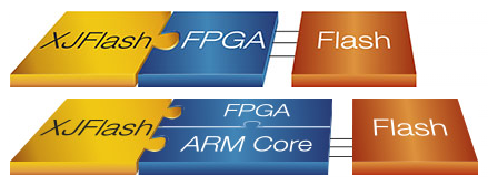
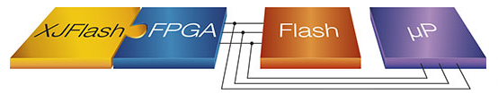
XJFlash is an FPGA-based advanced and innovative method that uses JTAG for high-speed in-system programming (ISP) of flash memories – all serial and parallel flash devices are supported. The most common use of XJFlash is programming the SPI/QSPI NOR flash used to configure an FPGA.
With XJFlash you can use the FPGA on your board to achieve flash programming speeds up to 50 times faster than those possible using conventional boundary scan techniques, often reaching the maximum speed for the flash memory.
Custom Solutions – Automatically Generated
XJFlash allows you to automatically generate customised programming solutions for the flash memory devices connected to FPGAs and FPGA SoCs (such as Xilinx Zynq® and Intel Cyclone® V) on your board.
The functional capabilities of the FPGA are harnessed to provide the fastest possible programming speeds. XJFlash automatically generates a custom design for each FPGA/flash combination, allowing you to achieve the best programming times, whilst not requiring you to do any FPGA development.*
If your flash memory is connected to an FPGA from Intel (Altera), Xilinx, Microsemi or Lattice, XJFlash uses the FPGA’s standard JTAG port to offer an in-circuit programming alternative to a SPI programmer or parallel flash programmer. XJFlash support all SPI modes (single-bit, dual, quad, QSPI, and octal) as well as parallel NOR flash devices.
*A licensed version of the relevant FPGA manufacturer’s tools will be required during the configuration of XJFlash. Free versions are sufficient for many devices.
Test Integration
XJFlash programming can be easily integrated into your XJTAG test system using XJDeveloper. All XJFlash programming can be run as part of an XJRunner boundary scan test project.
Configurable Flash Programming
It doesn’t matter whether you need to program a single flash memory device, or multiple devices that are connected in series, to expand the address space, or in parallel, to make a wider data bus, you can use XJFlash to speed up your programming operations.
Custom development
XJFlash can also be used for standalone programming requirements including direct access to I²C and SPI busses or custom protocols such as Microchips ICSP.
The required connections do not need to come from an FPGA on the target board. Providing the protocol signals are available on a header on that board, it should be possible to use XJFlash to achieve fast programming as part of an XJTAG solution.
XJFlash Example Timings
Minimum theoretical time for conventional boundary scan: 35 minutes.
Total XJFlash run time: 10.5 s to 32.6 s.
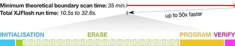
XJFlash will automatically step through four stages each time a flash device is programmed:
- Initialisation – The FPGA connected to the flash is configured with the XJFlash image required for the target board. Example time: 2.1 s.
- Erase – The flash can be erased using one of two algorithms. The basic erase will simply erase all blocks within a defined range (this may be the whole flash or just the space needed for the image to be programmed). The more intelligent erase will use the fact that it is quicker to read the flash than to erase it; as such it reads from each address and only starts erasing if some data is found. This step can be skipped if it is known that the flash will always be blank before it is programmed. Example time – intelligent erase enabled: 0.9 s with a device already erased, to 23 s with a fully programmed device (limited by erase time of device).
- Program – Data from the target images is streamed into the FPGA through its JTAG port. The FPGA then programs this data into the connected flash(s). Multiple files can be specified and programmed at defined offsets. This step can be bypassed if only verification is required. Example time: 6.2 s (limited by the programming speed of the device).
- Verify – The verification checks every byte in the flash against the specified file(s), ensuring there are no data bit errors. This step can be bypassed if only programming or erasing is required. Example time: 1.8 s with TCK at 10 MHz, reducing to 1.3 s with TCK at 20 MHz.
These example times are provided for a Spartan-6 XC6SLX9 programming a 2 MByte pseudorandom data file into the FPGA’s SPI configuration PROM.
Example Timings Using a Xilinx Zynq®-7000 series SoC
A 256 Mbit file can be programmed into a SPI NOR flash and verified in around 46 s, depending on the TCK speed and the memory type being used*; 32 Mbit of code takes just over 7 s.
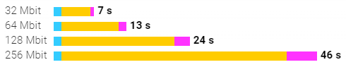
Adding an initial erase cycle adds only 3.1 s for an empty 256 Mbit flash, or 54 s for a full one. That drops to 0.4 s and between 6.5 and 9.2 s respectively for a 32 Mbit device.
* TCK = 66 MHz, pseudorandom data file. Time varies with flash type.
Example Timings Using a Xilinx Zynq® UltraScale+™ series SoC
A 256 Mbit file can be programmed into a SPI NOR flash and verified in around 42 s, depending on the TCK speed and the memory type being used**; 32 Mbit of code takes 7 s.
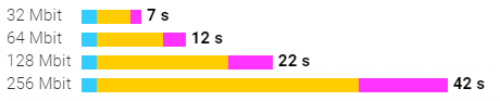
Adding an initial erase cycle adds only 2 s for an empty 256 Mbit flash, or 57 s for a full one. That drops to 0.3 s and 6.9 s respectively for a 32 Mbit device.
** TCK = 30 MHz, pseudorandom data file. Time varies with flash type.
Design requirements - Can I use XJFlash?
In order to use XJFlash all of the data, address and control signals on the flash device(s) must be connected to an FPGA on the target board. This can be a configuration PROM, or a flash device connected to any general purpose I/O pin. These connections can be direct, indirect, dedicated or shared: Direct connections – YES
Direct connections – YES
The flash is directly connected to the FPGA.
Indirect connections – YES

- The flash is connected to the FPGA via a buffer
- Some of the address signals are shared with the data signals and connected via a latch.
- There is another configurable device, such as a CPLD between the flash and the FPGA.
Shared connections – YES
The flash is connected to the FPGA in one of the modes described above but these connections are shared with another device (such as a processor).
No connections – YES (with design changes)

If your design contains an FPGA but the flash is not connected in any of the configurations described, it may be possible to use spare pins on the FPGA to establish connections to the flash. These connections would not be used in the mission mode of the board but would allow you to use XJFlash to perform fast flash programming. If your FPGA is already connected to the same address/data bus as the flash then this may not require many extra signals.
No FPGA – Not directly

Unfortunately, it is not possible to use XJFlash if there is no FPGA. However, if it is possible to bring the connections of the flash to a header or test points on the board, XJFlash fast programming can be used via those connections using an XJAccelerator card.
Alternatively, it may be possible to do fast flash programming using the debug interface on a processor – please contact us to see if you can use this approach on your board.
Supported FPGAs
Compatibility
- Intel (Altera) – Arria GX, Arria II GX, Arria II GZ, Arria V, Arria V GZ, Arria 10, Cyclone, Cyclone II, Cyclone III, Cyclone III LS, Cyclone IV E, Cyclone IV GX, Cyclone V, Stratix, Stratix GX, Stratix II, Stratix II GX, Stratix III, Stratix IV, Stratix V, Stratix 10
- Lattice – MachXO2, LatticeECP3, LatticeXP2
- Microsemi – IGLOO2, ProASIC3, ProASIC3E, ProASIC3L, SmartFusion2
- Xilinx – Artix-7, Kintex-7, Kintex UltraScale, Kintex UltraScale+, Spartan-3, Spartan-3A, Spartan-3E, Spartan-6, Spartan-7, Virtex-II, Virtex-II Pro, Virtex-4, Virtex-5, Virtex-6, Virtex-7, Virtex UltraScale, Virtex UltraScale+, Zynq-7000, Zynq UltraScale+
This list is continuously growing, so contact us for the latest details.
All trademarks are the property of their respective owners.
Recommended system requirements
- Intel® Core i3, i5, i7 processor or equivalent (any generation)
- Microsoft® Windows® 8, Windows 8.1, Windows 10 (1607 and later), or Windows 11 (32 or 64 bit)
- 4 GB of RAM
More Product Information

- Repair-focused environment for XJDeveloper / XJRunner tests.
- Full Connection test.
- RAM, Flash and other non-JTAG device tests.
- Flash, FPGA, CPLD and EEPROM programming.
- Layout Viewer* to show the physical location of faulty nets, pins and components.
- Schematic Viewer* to show the circuit design around faults.
- Direct control of the pins/balls of JTAG devices.
- View pin states graphically in real time or capture them in the Waveform Viewer.
- Trace signals to identify shorts, opens and other faults.

- Reduce flash programming times
- SPI, QSPI, parallel NOR flash devices supported
- Support for NAND flash devices available on request
- Shortened development cycles
- No need for additional equipment
- Can be used for fast firmware upgrade
- No FPGA development required
- Improve reliability of your boards by increasing analogue and digital test coverage
- Reduce your debug time by enhanced fault isolation
- XJTAG can reduce the cost and complexity of your custom test jigs
- Reach your devices on non-JTAG boards with ‘Black box’ testing
- Only BSDL files required to get the board up and running
- Set up pin states – e.g. low, high, toggling
- Trace shorts, opens and other signals
- Easy low-level access to device pins/busses
- Clear display of the pins/balls with variable zoom levels and split screen
- View JTAG chain data as waveforms
- Quickly find and monitor changing pins
- Program devices with SVF and STAPL files
- Real-time interaction
- XJIntegration (use XJAnalyser functionality from other software)
Highly scalable with unprecedented data transfer rates, the Hardware Isolation Platform is a dual-segment solution that combines cutting-edge security and adaptive capabilities to ensure guaranteed spacial isolation of critical data and optimize diverse workloads.
- Cross Domain Solution - Control comms and data transfer between domains of different classification levels with an FPGA hardware firewall.
- Data Isolation - Remote areas of memory create a data buffer between CPUs or virtual machines, securely storing frequently accessed data.
- Mixed Criticality - Integrate workloads with different criticalities on a single platform while prioritizing higher criticality tasks over lower ones.

- Support for the highest speeds available in CoaXPress 2.0
- Connect to and capture from up to four cameras or combine connections for even higher data rates
- Simplify cabling with PoCXP support between cameras and vision computer
- Offload host computer of custom image processing using a field-programmable gate array (FPGA) device
- Distribute image processing workload across multiple computers through data forwarding capability
- Synchronize with sensors, encoders, and controllers with ample auxiliary I/Os for each CoaXPress connection
- Use license fingerprint for Aurora Imaging Library and avoid the need for a separate hardware key
- Monitor and troubleshoot acquisition performance in detail using Aurora Gecho event-logging tool

- Small, lightweight, portable design: ideal for lab and field work
- Self-contained licence so you can use the XJTAG system on multiple PCs
- Re-configurable unit for multiple UUTs saving costs

- Support the most high-performance Camera Link cameras with available support for Full and 80-bit mode at up to 85 MHz
- Perform deterministic image acquisition by way of the jitter-free Camera Link 2.1 interface
- Offload host computer of custom image processing using a field-programmable gate array (FPGA) device
- Eliminate missed frames through a PCIe® 2.0 x8 host interface and ample onboard buffering
- Optimize multi-camera applications via support for up to four Base or two Full/80-bit Camera Link cameras per board
- Minimize space requirements and maximize PC compatibility through a half-length design with mini Camera Link connectivity for true single-slot operation
- Improve and simplify system connectivity with Power-overCamera-Link (PoCL) support at extended cable lengths
- Reduce your time spent debugging boards due to high precision fault isolation
- Improve your time to market and reduce project risk by early design verification
- Reduce your test development time by reusing tests from prototype/design in manufacturing and field support
- Ongoing time savings by test reuse across projects
XJTAG
XJTAG is a world leading supplier of JTAG boundary-scan software and hardware tools. The company focuses on innovative product development and high-quality technical support. XJTAG products use IEEE Std.1149.x (JTAG boundary-scan) to enable engineers to debug, test and program electronic circuits quickly and easily. This can significantly shorten the electronic design, development and manufacturing processes. XJTAG is based in Cambridge, UK, and its products are used globally by a wide range of industries. XJTAG is part of Cambridge Technology Group.
Contact Details
XJTAG CamTech House - UK Headquarters
137 Cambridge Road Ind. Est., Milton, Cambridge, CB24 6AZ, United Kingdom
Email: enquiries@xjtag.com
Test & Measurement
Download Line Card
Document

Embedded
Download Line Card
Document