You design the future. We help you make it happen.
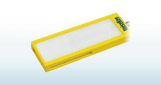
FormFactor - Cascade High Current Probe - Test power devices on wafer with high-performance and low-contact resistance on smaller pads
- Enables wafer probing up to 100 A pulsed and 10A DC
- Innovative multi-fingertip design provides even distribution of current
- Supports up to 500 V
- Replaceable Tungsten probe tips
- Temperature range of -60°C to 300°C
- Minimal contact resistance at the pad-tip junction to reduce heating during measurements, with fewer probe marks
- Prevents against thermal runaway
- Measure devices on wafer at higher currents than ever before
- Small scrub minimizes damage to aluminum pad
- Small footprint – tip fits on a 1 mm pad
Designed specifically for testing power devices on wafer, the HCP probe reduces probe and device destruction at high currents by minimizing contact resistance at the wafer-to-probe interface to prevent device heating at the tip. The innovative multi-finger design distributes the current over multiple contact points at the tip and is joined by a single heatsink which pulls heat from the probe tip.
More Product Information
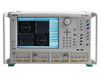
- SPA available from 70KHz to 20/40/70/110/125/145 and 220GHz. Also available for banded configuration to 1.1THz.
- Dual SPA mode available: suitable for Mixers/Amplifier/ Harmonics /Spurious testing.
- SPA available on all ports. User can define which port to use as SPA port.
- Several detection types available in classical mode: Peak, minimum, RMS, Mean.
- Various math functions can be applied on SPA mode like Min hold/max hold/ user defined equations.
- Sources and receivers can be independently configured. Can be used as Tracking Generator.
- For units that have a dual source, a dual drive option is available. Support for external source control also possible.
- Phase synchronization for units with Dual source available. This feature allows users to control and configure the phase between the two sources.
- Source and receiver attenuator available with VNA can be activated in SPA mode. Recommendation to use option 62 (with attenuator on receiver side) for measuring the spectrum content of high-power devices.
- Software option: easy to install and upgrade existing user equipment.
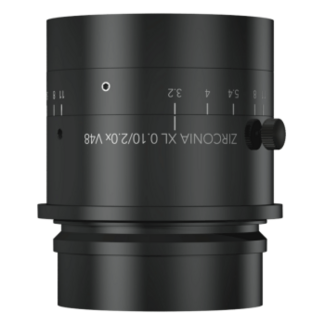
- Image circle: 62.5 mm - 82 mm
- High resolution down to 5µm pixel size
- Optimized for specific magnifications
- 6 magnifications available: 0.1x - 2.0x
- Version with beamsplitter available
- Best azimuth marking
- V48-Mount for easy installation

-
Combination of DC and RF in a single probe module: One dual probe or a maximum of three RF; a maximum of 9 DC standard (other quantities upon request).
-
Utilizes ACP tip design, GSG, GS or SG
-
RF tips available from DC to 110 GHz
-
Choice of BeCu or tungsten tips
-
DC power needles come standard with 100 pF microwave capacitor
-
Power bypass inductance: 8 nH
-
Maximum DC voltage: 50 V without power bypassing (25 V with standard power bypassing, and component dependent with custom power bypassing)
-
Ideal for probing the entire circuit for functional test
-
Dual ACP configuration supports differential signaling applications
-
DC probes can provide power or slow logic to circuit under test

- Support the most high-performance Camera Link cameras with available support for Full and 80-bit mode at up to 85 MHz
- Perform deterministic image acquisition by way of the jitter-free Camera Link 2.1 interface
- Offload host computer of custom image processing using a field-programmable gate array (FPGA) device
- Eliminate missed frames through a PCIe® 2.0 x8 host interface and ample onboard buffering
- Optimize multi-camera applications via support for up to four Base or two Full/80-bit Camera Link cameras per board
- Minimize space requirements and maximize PC compatibility through a half-length design with mini Camera Link connectivity for true single-slot operation
- Improve and simplify system connectivity with Power-overCamera-Link (PoCL) support at extended cable lengths
- High performance GPS disciplined Time/Frequency standard
- Ethernet Interface for management and control
- Network Time Protocol (NTP)
- Multiple 1PPS outputs with individual delay compensation
- Multiple Low Phase Noise 10MHz outputs with software programmable level
- Time Code outputs including Have Quick, IRIG A, IRIG B, IRIG E, IRIG G
- Sync to GPS or to Have Quick/1PPS per ICD-GPS-060
- Choice of internal disciplined OCXO or Rubidium Oscillator
- Qualified for Harsh Environment: DO-160, MIL-STD-704, -461, -810
- Designed to Minimize Obsolescence Risk & Management: FPGA-Based Design
- Easy Set up: User-Defined Media Partitioning
- Multi-Protocol, GigE Interfaces: FTP, NFS, SMB/CFS, HTTP
- High-Capacity Rugged Removable Cartridge: 64GB to 2TB

- Revolutionary technology advancement for wafer and die-level photonics probing
- Real-time in-situ calibrations
- Singulated die testing
- True die-level edge coupling
- In-situ power measurements
- Advanced calibration technologies
- Enables autonomous measurements
See "Specifications & Details" tab for more key features
The Broadband sleeve antenna was developed to efficiently perform proximity radiation immunity testing.
The international standards ISO11451-3/ISO11452-9 stipulate proximity radiation immunity testing methods that assume electromagnetic interference when wireless transmitters such as smartphones and Wi-Fi devices are placed in close proximity to other electronic devices.
This product is a small, lightweight, high-gain antenna used in these standards that covers a wide bandwidth and has good radiation characteristics. Since it can be used in the wide band from 5GHz to 8GHz, it can be used to perform proximity radiation immunity testing assuming wireless LAN in the 6GHz band (up to 7.125GHz).
- High power density in 4U/14U chassis up to 36 kVA.
- Intuitive touch panel control.
- iX2™ current doubling technology.
- Multi-language user interface for global operation.
- Auto paralleling for higher power.
- Combine units for multi-phase configurations
- Complete optional avionic test suites.
- ATE version available
FormFactor, Inc.
Website
FormFactor, Inc. (NASDAQ:FORM) is a leading provider of essential test and measurement technologies along the full IC life cycle – from characterization, modeling, reliability, and design de-bug, to qualification and production test.
We constantly strive to help our customers solve the advanced test and measurement challenges of the broader semiconductor industry. Our focus on customer partnership, innovation, agility and operational excellence allows us to earn sustainable business every day.
