You design the future. We help you make it happen.
FormFactor, Inc. (NASDAQ:FORM) is a leading provider of essential test and measurement technologies along the full IC life cycle – from characterization, modeling, reliability, and design de-bug, to qualification and production test.
We constantly strive to help our customers solve the advanced test and measurement challenges of the broader semiconductor industry. Our focus on customer partnership, innovation, agility and operational excellence allows us to earn sustainable business every day.
Contact Details
FormFactor, Inc. Corporate Headquarters
7005 Southfront Road, Livermore, CA 94551, USA
Phone: 925-290-4000
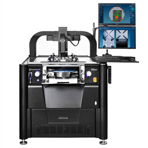
Test & Measurement
Download Line Card

Products

-
Best price per contact – typically over one million (1,000,000) touchdowns
-
RF/Microwave signal is shielded and completely air isolated in the probe body
-
Excellent performance in vacuum environments and temperatures as low as 4 K, or as high as 300°C
-
Highest impedance control with perfectly-symmetrical, MEMS-machined coplanar contact structure
-
Probe on any pad material with minimal damage

-
Replace costly and inflexible test fixtures with easy-to-use probe tips
-
Long lifetime – typically over 1,000,000 contacts
-
GS/SG footprint up to 4 GHz and GSG up to 20 GHz
-
High-power RF test: up to 30 Watts
-
Test at temperatures from -60°C to 200°C

-
High power – 66 W at 2.4 GHz and 43 W at 5 GHz
-
Extremely low insertion loss of ≤ 0.4 dB (typical) up to 40 GHz
-
Excellent contact control and low contact resistance
-
High performance on any pad material (Al or Au)
-
Longest lifetime – typically one million (1,000,000) touchdowns

-
Unique Air Coplanar tip design with choice of beryllium copper (BeCu) or tungsten tip material
-
DC to 110 GHz models available in single and dual line versions
-
Low insertion and return loss with ultra-low-loss ( -L ) versions
-
Excellent crosstalk characteristics
-
Wide operating temperature -65 ° C to + 200 ° C
-
Wide range of pitches available, from 50 to 1250 µm
-
Individually supported contacts
-
Reduced contact (RC) probe tips for small pads
-
BeCu tip provides rugged, repeatable contact on gold pads

-
Functional temperature range of -263 to +150°C
-
Stainless steel tip material for thermal decoupling
-
Coaxial cable with TCE matched inner and outer conductors
-
Consistent tip geometry even at cryogenic temperatures

-
Combination of DC and RF in a single probe module: One dual probe or a maximum of three RF; a maximum of 9 DC standard (other quantities upon request).
-
Utilizes ACP tip design, GSG, GS or SG
-
RF tips available from DC to 110 GHz
-
Choice of BeCu or tungsten tips
-
DC power needles come standard with 100 pF microwave capacitor
-
Power bypass inductance: 8 nH
-
Maximum DC voltage: 50 V without power bypassing (25 V with standard power bypassing, and component dependent with custom power bypassing)
-
Ideal for probing the entire circuit for functional test
-
Dual ACP configuration supports differential signaling applications
-
DC probes can provide power or slow logic to circuit under test

-
Ease of use – Less experienced operators can perform DC measurements by simply pushing a button. This reduces the need of experienced users full time on each system.
-
Reduced Soak Time – The system will automatically re-align the probes to the pads if they drift from alignment. This reduces test time and increases throughput.
-
Unattended Use – Measurements can be left running over night or the weekend, testing all devices on the wafer, and at different temperatures without the need of an operator.

-
Ease of use – Less experienced operators can perform an RF calibration up to 500 GHz by simply pushing a button. This reduces the need of experienced users full time on each system.
-
Reduced Soak Time – The system will automatically re-align the probes to the pads if they drift from alignment. This reduces test time and increases throughput.
-
Unattended Use – Measurements can be left running over night or the weekend, testing all devices on the wafer, and at different temperatures without the need of an operator.
-
Calibration Monitor and Re-calibration – System will continuously monitor calibration drift, and automatically re-calibrate the system should the drift exceed a predefined limit.

- Revolutionary technology advancement for wafer and die-level photonics probing
- Real-time in-situ calibrations
- Singulated die testing
- True die-level edge coupling
- In-situ power measurements
- Advanced calibration technologies
- Enables autonomous measurements
See "Specifications & Details" tab for more key features

Flexibility
- Application flexibility: Coax, Triax, RF/mmW, High Power, Double Sided
- Temperatures range from -60°C to +300°C
- Surfaces are nickel or gold-plated
- Hybrid chuck design – operation with and without cooling unit
- Field-upgradeable: On-site cold upgrades for all main prober platforms
Highest Efficiency for Reduced Cost of Test
- Up to 25% lower air consumption (CDA) than other systems on the market with no compromise in transition times
- Up to 15% faster transition times than other systems on the market
Flexibility
- DC, AC and RF/microwave device characterization, 1/f, WLR, FA and design debug
- Full thermal range of -60°C to +300°C
- Compatible with TopHat or IceShield
- Usage of manual and motorized positioners, probe cards within EMI-shielded environment
- Upgrade path to meet your future needs
- Stable and repeatable measurements over a wide thermal range
High accuracy and repeatability
- Reliable and repeatable contact
- Moisture-free, light-tight and EMI-shielded test environment with MicroChamber® technology
- Advanced EMI-shielding with PureLine and AttoGuard technologies available
- Superior low-leakage and low-noise measurements
- Safe and accurate hands-off testing
- Minimizes settling times for efficient measurements over full thermal range
See "Specifications & Details" tab for more key features

OptoVue
- Revolutionary technology advancement for wafer and die-level photonics probing
- Real-time in-situ calibrations
- Singulated die testing
- True die-level edge coupling
- In-situ power measurements
- Advanced calibration technologies
- Enables autonomous measurements
Horizontal Die-Level Edge Coupling
- Highest accuracy in test results
- Lowest coupling loss
- Repeatable measurement results due to exclusive automated fiber-to-facet alignment technology
- Reduced risk of damaging fibers with collision avoidance technology
- Ease of use for less experienced users
- Enables close simulation of real-world conditions with device performance closest to the final application
See "Specifications & Details" tab for more key features