FormFactor - Cascade |Z| Probe® PCB - Robust RF test on PCB and ceramic
-
Replace costly and inflexible test fixtures with easy-to-use probe tips
-
Long lifetime – typically over 1,000,000 contacts
-
GS/SG footprint up to 4 GHz and GSG up to 20 GHz
-
High-power RF test: up to 30 Watts
-
Test at temperatures from -60°C to 200°C
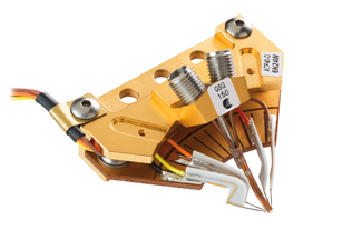
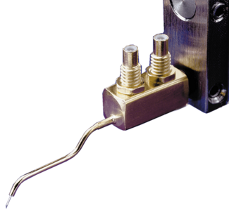
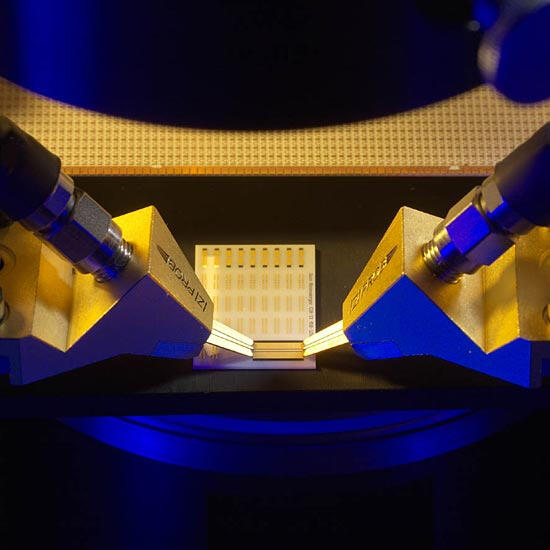
Flexibility is the key for efficient PCB and ceramic testing. The |Z| Probe® PCB is simple to align and handle and can be easily positioned. It optimally replaces costly test fixtures which are often inflexible. A robust design makes the |Z| Probe PCB easy to handle and offers a long working life typically more than one million (1,000,000) contacts.
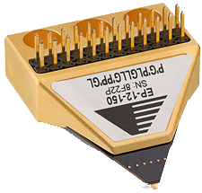
The planar tip of the |Z| Probe PCB has precisely calculated, parallel, separate contact springs which move independently of one another, allowing a precise, quick and simple contact with the DUT, even if there are significant contact height differences. This unique feature as well as the overall very robust design of the |Z| Probe PCB ensures a long life and simple handling.
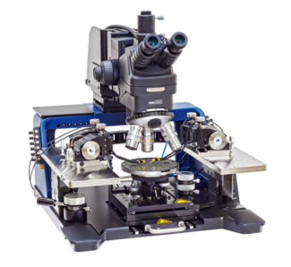
Used in conjunction with a manual probe system including probe positioners and calibration substrates, the |Z| Probe PCB becomes the ultimate tool for all RF circuit probing needs.
More Product Information

Flexibility
- DC, AC and RF/microwave device characterization, 1/f, WLR, FA and design debug
- Full thermal range of -60°C to +300°C
- Compatible with TopHat or IceShield
- Usage of manual and motorized positioners, probe cards within EMI-shielded environment
- Upgrade path to meet your future needs
- Stable and repeatable measurements over a wide thermal range
High accuracy and repeatability
- Reliable and repeatable contact
- Moisture-free, light-tight and EMI-shielded test environment with MicroChamber® technology
- Advanced EMI-shielding with PureLine and AttoGuard technologies available
- Superior low-leakage and low-noise measurements
- Safe and accurate hands-off testing
- Minimizes settling times for efficient measurements over full thermal range
See "Specifications & Details" tab for more key features

-
Combination of DC and RF in a single probe module: One dual probe or a maximum of three RF; a maximum of 9 DC standard (other quantities upon request).
-
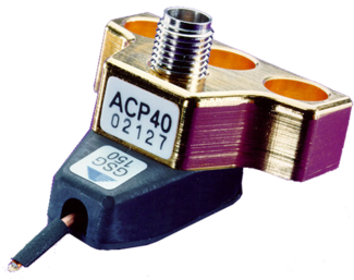
Utilizes ACP tip design, GSG, GS or SG
-
RF tips available from DC to 110 GHz
-
Choice of BeCu or tungsten tips
-
DC power needles come standard with 100 pF microwave capacitor
-
Power bypass inductance: 8 nH
-
Maximum DC voltage: 50 V without power bypassing (25 V with standard power bypassing, and component dependent with custom power bypassing)
-
Ideal for probing the entire circuit for functional test
-
Dual ACP configuration supports differential signaling applications
-
DC probes can provide power or slow logic to circuit under test

Optimized Measurement Setup
- Multi-purpose SIGMA instrument integration kit
- Shorter cabling and universal chuck connection
- Triax probe with protected guard
- Optimized signal path
- Safe probe tip exchange
- Seamless integration of various analyzers
High Power Chuck
- Triax design for low-leakage measurements up to 3 kV
- Special chuck surface coating
- High-isolation ready
- High-current measurement up to 100 A with lowest contact resistance
- Optional upgrade for 10 kV (coax) operating voltage
- Thin wafer handling capability
Safe Operation
- Arcing protection
- Shield Enclosure with interlock
- Advanced grounding concept
- Maximum protection from high-voltage shock for users and devices
- Common ground protection for all instruments
- EMI/light-tight shielded environment

- Lithographic thin-film construction
- Excellent crosstalk characteristics
- Non-oxidizing nickel alloy tips
- Innovative force delivery mechanism
- 40GHz, 50GHz, 67GHz, 110GHz and 145GHz connectors available
- GSG, SG, GS, GSGSG, GSSG, SGS configurations
- 50 to 250 µm pitches (other pitches available on request)
- High current version (2 A) available
Advantages
- Superior field confinement reduces unwanted couplings to nearby devices and transmission modes
- Superior measurement accuracy and repeatability
- Small scrub minimizes damage to aluminum pad
- Typical contact resistance < 0. 05 Ω on Al, <0.02Ω on Au
- Save valuable wafer space and reduce pad parasitics by being able to shrink pad geometries to 25 x 35 µ m (best case)

The LWP series Lightwave Probe enables optical measurements for on-wafer and hybrid photonics devices. It features user replaceable fiber pigtails allowing the probe to be optimized for a variety of light delivery and light collection applications including the characterization of topside illuminated photodiodes, Vertical Cavity Surface Emitting Lasers (VCSELs), hybrid transmitters and receivers, and LEDs.

The CSR family of calibration substrates delivers the highest accuracy available due to the high quality of each substrate. The calibration standards are manufactured using rugged, hard gold, which ensures a long lifetime.

-
Replace costly and inflexible test fixtures with easy-to-use probe tips
-
Long lifetime – typically over 1,000,000 contacts
-
GS/SG footprint up to 4 GHz and GSG up to 20 GHz
-
High-power RF test: up to 30 Watts
-
Test at temperatures from -60°C to 200°C

- Probe loss is 3 dB typical between 140 and 200 GHz, S11/S22 15 dB typical
- Reduced unwanted couplings and transmission modes
- Able to shrink pad geometries to 25 x 35 µm (best case)
- Typical contact resistance < 0.05 Ω on Al, < 0.02 Ω on Au
- WR15, WR12, WR10, WR8, WR6, WR4, WR3, and WR2 bands available.

Flexibility
- Different substrate carriers for wafers up to 100 mm or single dies
- Up to six positioners
- Use with liquid nitrogen or helium, depending on the target temperature
- Probing with an open chamber lid possible under atmospheric condition
- Specially designed for laboratory environments
- Covers wide range of measurements (I-V, C-V, RF, MEMS, OPTO)
See "Specifications & Details" tab for more key features

FormFactor, Inc.
FormFactor, Inc. (NASDAQ:FORM) is a leading provider of essential test and measurement technologies along the full IC life cycle – from characterization, modeling, reliability, and design de-bug, to qualification and production test.
We constantly strive to help our customers solve the advanced test and measurement challenges of the broader semiconductor industry. Our focus on customer partnership, innovation, agility and operational excellence allows us to earn sustainable business every day.
Contact Details
FormFactor, Inc. Corporate Headquarters
7005 Southfront Road, Livermore, CA 94551, USA
Phone: 925-290-4000
Test & Measurement