You design the future. We help you make it happen.
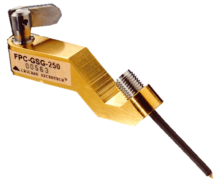
FormFactor - Cascade FPC Probe - Rugged, deep reach RF probing for modules and circuit boards
- DC-40 GHz bandwidth
- 10 ps rise time
- Low insertion and return loss
- 2 mils of tip-to-tip compliance
- High probing angle and clearance
The FPC probe is a high frequency 50 ohm coaxial probe that offers a signal line with either one or two low-inductance fixed-pitch ground contacts. The probe tip structure is lithographically defined for unsurpassed impedance control, preserving the highest integrity possible when launching and receiving signals from SMT boards, hybrids and multi-chip modules(MCM).
Advantages
- Maintains 50-ohm environment which allows accurate high-frequency measurement of microelectronic modules
- Compliant tips allow probing of non-planar structures
- BeCu tips provide longer probing life and reduce probe damage
- Access contacts close to components, module walls, or other obstructions
Document
More Product Information
Flexibility
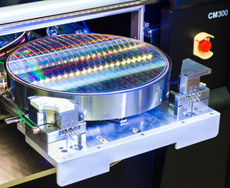
- Application flexibility: Coax, Triax, RF/mmW, High Power, Double Sided
- Temperatures range from -60°C to +300°C
- Surfaces are nickel or gold-plated
- Hybrid chuck design – operation with and without cooling unit
- Field-upgradeable: On-site cold upgrades for all main prober platforms
Highest Efficiency for Reduced Cost of Test
- Up to 25% lower air consumption (CDA) than other systems on the market with no compromise in transition times
- Up to 15% faster transition times than other systems on the market
Flexibility
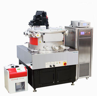
- Different substrate carriers for wafers up to 200 mm or single dies
- Probe cards and/or up to eight positioners
- Optional thermal chuck (-60°C to 300°C) and pressure regulation
- Accessories available, such as black bodies and optical motion analysis tools
- Optional upgrade for 300 mm wafer
- Designed for industrial environments
- Covers wide range of measurements (I-V, C-V, RF, MEMS, OPTO)
- Ideal for small structures
See "Specifications & Details" tab for more key features
-
Functional temperature range of -263 to +150°C
-
Stainless steel tip material for thermal decoupling
-
Coaxial cable with TCE matched inner and outer conductors
-
Consistent tip geometry even at cryogenic temperatures
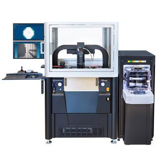
Gold-plated TESLA High-power MicroVac™ Chucks
- Prevent thin wafers from curling and breaking
- Advanced MicroVac chuck surface for minimum contact resistance between wafer and chuck
- Accurate Rds(on) measurement at high current
- Accurate UIS measurements at high temperature
See "Specifications & Details" tab for more key features
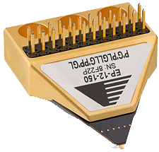
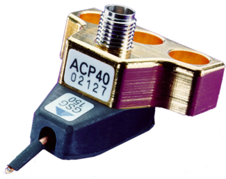
- High performance power bypassing provides low-impedance and resonant-free connections to 20 GHz
- RF bandwidth to 500 MHz
- Long probe life: > 250,000 contacts
- Beryllium-copper tips for gold pads or tungsten for aluminum pads
- Oscillation-free testing of wide-bandwidth analog circuits
- Use with ACP series probes to provide functional at-speed testing for known-good-die
- Mix multiple contact types: Ground, Power (Standard or Eye-Pass), Logic/Signal
- Low and repeatable contact resistance on aluminum pads ( < 0.25 Ω on Al, < 0.01 Ω on Au)
-
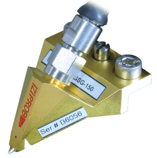
High power – 66 W at 2.4 GHz and 43 W at 5 GHz
-
Extremely low insertion loss of ≤ 0.4 dB (typical) up to 40 GHz
-
Excellent contact control and low contact resistance
-
High performance on any pad material (Al or Au)
-
Longest lifetime – typically one million (1,000,000) touchdowns
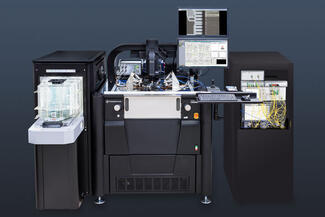
OptoVue
- Revolutionary technology advancement for wafer and die-level photonics probing
- Real-time in-situ calibrations
- Singulated die testing
- True die-level edge coupling
- In-situ power measurements
- Advanced calibration technologies
- Enables autonomous measurements
Horizontal Die-Level Edge Coupling
- Highest accuracy in test results
- Lowest coupling loss
- Repeatable measurement results due to exclusive automated fiber-to-facet alignment technology
- Reduced risk of damaging fibers with collision avoidance technology
- Ease of use for less experienced users
- Enables close simulation of real-world conditions with device performance closest to the final application
See "Specifications & Details" tab for more key features
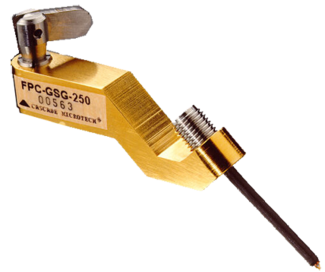
- DC-40 GHz bandwidth
- 10 ps rise time
- Low insertion and return loss
- 2 mils of tip-to-tip compliance
- High probing angle and clearance
High-voltage/current Probes
- On-wafer power device characterization up to 10,000 V DC / 600 A
- Reduced probe and device destruction at high currents up to 20 A DC and 300 A pulse
- Increased isolation resistance and dielectric strength to provide full triaxial capability at high voltage (3,000 V) for low-leakage measurement

FormFactor, Inc.
Website
FormFactor, Inc. (NASDAQ:FORM) is a leading provider of essential test and measurement technologies along the full IC life cycle – from characterization, modeling, reliability, and design de-bug, to qualification and production test.
We constantly strive to help our customers solve the advanced test and measurement challenges of the broader semiconductor industry. Our focus on customer partnership, innovation, agility and operational excellence allows us to earn sustainable business every day.