You design the future. We help you make it happen.
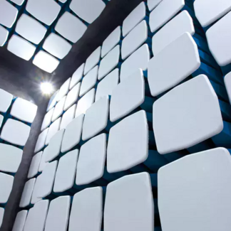
FormFactor - Cascade Shield Enclosure Light-tight probing
- Light-tight version and EMI-shielded version for low noise and light-sensitive measurements
- Application flexibility, ideal for use in high frequency applications
- Sized to accommodate thermal chucks, laser cutter, and video equipment on the probe system
- Suitable for integration with vibration isolating tables
Shield Enclosures are designed for durable stability and sized to accommodate analytical probers equipped with all kinds of accessories, including thermal chucks, laser cutters, TV and emission cameras. The EMI-shielded version guarantees a light-tight and electromagnetically shielded environment for all sensitive measurements.
More Product Information

All tools in one belt
- Calibration
- Validation
- Measurement
- Analysis
Advanced functionality
- Multi-Port Hybrid Cals
- Enhanced Verification and Reports
- Post Processing and Sequencing
Get started
- Guided wizards and multimedia tutorials integrated
- Intelligence in setups
Flexible setups
- Standalone for manual probe stations
- Fully integrated in Velox Probe station control software
- Workspaces to build custom configurations that include selected combinations of system setup files, calibration setup files, and reports
- Support of more than 24 of the most common VNA’s

- Designed for use with specific Probe Systems
- Tables to suit all facility requirements and applications
- Stable probing, even in submicron range
- Granite platen ensures rigidity and temperature stability
- Can be combined with the Shield Enclosures

Flexibility
- Different substrate carriers for wafers up to 200 mm or single dies
- Probe cards and/or up to eight positioners
- Use with liquid nitrogen or helium, depending on the target temperature. Or use of cryo-cooler for dry-cooling option.
- Accessories available, such as black bodies and optical motion analysis tools
- Optional upgrade for 300 mm wafer
- Designed for industrial environments
- Covers wide range of measurements (I-V, C-V, RF, MEMS, OPTO)
- Ideal for small structures
See "Specifications & Details" tab for more key features

- Coaxial and triaxial measurements up to 10,000 V
- High-quality construction with low-noise electrical performance
- Replaceable probe tips in a variety of tip sizes
- Temperature range of of -60°C to 300°C
- Triaxial measurement ensures a much better understanding of device leakage in the off state
- Highly reliable, stable and repeatable measurements
- Integrally designed as part of a complete measurement solution
Very useful where space is restricted, the EMC chamber EMC-MC will settle into almost any office space. Its small overall size results from the use of our modular SmartShield chamber lined with our AEPH HyPyr-LossTM absorber technology requiring less volumetric space than in a traditional chamber. This mini compact EMC chamber is applicable in EMC pre compliance and general Research & Development RF testing.

-
Functional temperature range of -263 to +150°C
-
Stainless steel tip material for thermal decoupling
-
Coaxial cable with TCE matched inner and outer conductors
-
Consistent tip geometry even at cryogenic temperatures

-
Ease of use – Less experienced operators can perform an RF calibration up to 500 GHz by simply pushing a button. This reduces the need of experienced users full time on each system.
-
Reduced Soak Time – The system will automatically re-align the probes to the pads if they drift from alignment. This reduces test time and increases throughput.
-
Unattended Use – Measurements can be left running over night or the weekend, testing all devices on the wafer, and at different temperatures without the need of an operator.
-
Calibration Monitor and Re-calibration – System will continuously monitor calibration drift, and automatically re-calibrate the system should the drift exceed a predefined limit.

High flexibility
- Re-configurable for DC, RF, mmW, FA, WLR and more
- Thermal range: -60˚C to 300˚C available
- Upgrade path to meet your future needs
- Stable and repeatable measurements over a wide thermal range
See "Specifications & Details" tab for more key features

-
On-Off power switch
-
15 A Circuit Breaker
-
Inlet - IEC C14 for use with any cordset
-
Outlets – (8) IEC C13
Test Tap:
-
3ft.
-
(2) fork terminals (current)
-
(1) fork terminals (ground)
-
(2) Shielded Banana (voltage)
FormFactor, Inc.
Website
FormFactor, Inc. (NASDAQ:FORM) is a leading provider of essential test and measurement technologies along the full IC life cycle – from characterization, modeling, reliability, and design de-bug, to qualification and production test.
We constantly strive to help our customers solve the advanced test and measurement challenges of the broader semiconductor industry. Our focus on customer partnership, innovation, agility and operational excellence allows us to earn sustainable business every day.
