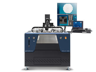
You design the future. We help you make it happen.
FormFactor - Cascade ACP Probe – Cryo/Vacuum - Superior mechanical properties at cryogenic temperatures
-
Functional temperature range of -263 to +150°C
-
Stainless steel tip material for thermal decoupling
-
Coaxial cable with TCE matched inner and outer conductors
-
Consistent tip geometry even at cryogenic temperatures
Designed to provide superior mechanical properties at cryogenic temperatures while maintaining solid RF measurement performance. Functional temperature range of -263 to + 150 ° C. Consistent tip geometry even at cryogenic temperatures.
More Product Information

- High-quality construction with low-noise electrical performance
- Kelvin version for convenient 4-point measurements
- Replaceable coaxial probe tips, with choice of tip radii, and full electrical guard to the probe tip
- SSMC 50 connectors
- Ultra-low, fA and fF measurements from -65 º C to 150 º C
- Mechanical Platen Lift: Enhances safety during complex RF set-ups, increasing operator confidence and minimizing the risk of errors.
- Ease of Use and Advanced Automation: Fully compatible with FormFactor’s Autonomous RF and DC measurement assistants, as well as Velox Dash™ companion app control.
- Reconfigurable Platen Inserts: Quickly switch between TopHat, PCH, and IceShield inserts within minutes to support a wide variety of test configurations.
- Spacious Platen Design: Provides flexibility for both RF and DC setups without space limitations, ensuring easy integration of different configurations.
- Compact Design: Small footprint with field-upgradable components for smooth integration into existing test cells.
- Low-Volume MicroChamber and FemtoGuard Thermal Triaxial Chuck: Included by default

All tools in one belt
- Calibration
- Validation
- Measurement
- Analysis
Advanced functionality
- Multi-Port Hybrid Cals
- Enhanced Verification and Reports
- Post Processing and Sequencing
Get started
- Guided wizards and multimedia tutorials integrated
- Intelligence in setups
Flexible setups
- Standalone for manual probe stations
- Fully integrated in Velox Probe station control software
- Workspaces to build custom configurations that include selected combinations of system setup files, calibration setup files, and reports
- Support of more than 24 of the most common VNA’s

-
High power – 66 W at 2.4 GHz and 43 W at 5 GHz
-
Extremely low insertion loss of ≤ 0.4 dB (typical) up to 40 GHz
-
Excellent contact control and low contact resistance
-
High performance on any pad material (Al or Au)
-
Longest lifetime – typically one million (1,000,000) touchdowns

SlimVue Microscope
- Combined eye-pieces and CCD camera mount
- 3x zoom and quick lens exchange
- Quick lens exchange
- 1 um optical resolution
- Minimized scope footprint
- Fast change from navigation optics to high-resolution optics
- Resolving ‹ 50 μm pads
- Simple integration with any mmW modules
Application Specific Sigma Kits
- Engraved guides on mmW platen
- Supports broadband, load pull, coax RF and banded waveguide configuration
- Optical feedback on platen position (gauge)
- Adaptable to any mmW/sub-THz applications
- Seamless integration with any mmW modules and tuners
- Fast mounting and setup change
THz measurement capability
- Rock-solid mechanical design
- Submicron stage accuracy
- Optical feedback on platen and probe position (gauge)
- Motorized positioner
- <+-1 um separation repeatability
- Micrometer-accurate and repeatable probe placement and overtravel
- Highly-precise and stable THz measurements

Flexibility
- Different substrate carriers for wafers up to 200 mm or single dies
- Probe cards and/or up to eight positioners
- Optional thermal chuck (-60°C to 300°C) and pressure regulation
- Accessories available, such as black bodies and optical motion analysis tools
- Optional upgrade for 300 mm wafer
- Designed for industrial environments
- Covers wide range of measurements (I-V, C-V, RF, MEMS, OPTO)
- Ideal for small structures
See "Specifications & Details" tab for more key features

-
Unique Air Coplanar tip design with choice of beryllium copper (BeCu) or tungsten tip material
-
DC to 110 GHz models available in single and dual line versions
-
Low insertion and return loss with ultra-low-loss ( -L ) versions
-
Excellent crosstalk characteristics
-
Wide operating temperature -65 ° C to + 200 ° C
-
Wide range of pitches available, from 50 to 1250 µm
-
Individually supported contacts
-
Reduced contact (RC) probe tips for small pads
-
BeCu tip provides rugged, repeatable contact on gold pads

Superior Mechanics
- Highly stable granite base
- Independent, coarse movement of X and Y axes, combined with easy fine adjustments
- Excellent measurement accuracy and repeatability
- Fast navigation and high-precision probe positioning
See "Specifications & Details" tab for more key features

- High performance power bypassing provides low-impedance and resonant-free connections to 20 GHz
- RF bandwidth to 500 MHz
- Long probe life: > 250,000 contacts
- Beryllium-copper tips for gold pads or tungsten for aluminum pads
- Oscillation-free testing of wide-bandwidth analog circuits
- Use with ACP series probes to provide functional at-speed testing for known-good-die
- Mix multiple contact types: Ground, Power (Standard or Eye-Pass), Logic/Signal
- Low and repeatable contact resistance on aluminum pads ( < 0.25 Ω on Al, < 0.01 Ω on Au)
FormFactor, Inc.
Website
FormFactor, Inc. (NASDAQ:FORM) is a leading provider of essential test and measurement technologies along the full IC life cycle – from characterization, modeling, reliability, and design de-bug, to qualification and production test.
We constantly strive to help our customers solve the advanced test and measurement challenges of the broader semiconductor industry. Our focus on customer partnership, innovation, agility and operational excellence allows us to earn sustainable business every day.

