You design the future. We help you make it happen.
FormFactor - Cascade Ultra High-Power (UHP) - Enabling single-contact high-current/high-voltage test
- Enables coaxial measurements up to 10,000 V and 300 A pulsed (600 A in a parallel configuration) with a single touchdown
- Even distribution of high current with innovative multi-fingertip design
- Compatible with TESLA 200/300 mm power device characterization system
- Reduced measurement time by testing both high-voltage and high-current conditions with a single touchdown
- Accurate characterization of a wide range of pad sizes and test currents, with minimum pad damage and contact resistance
- Safe, reliable and repeatable high-current/voltage measurements over a wide temperature range (from -55°C to +300°C)
FormFactor’s Ultra-High-Power Probe (UHP), a high-voltage parametric probe, handles both high voltage (up to 10,000 V) and high current (up to 600 A) at a wide temperature range (-60ºC to 300ºC).
The high pulse current achieves full I-V characterization with one setup and one touchdown. Together with a TESLA on-wafer power device characterization system, the UHP fully utilizes the high-voltage/current capability of Keysight B1505A and N1265A Ultra High Current Expanders.
Document
Document
More Product Information

Superior Mechanics
- Highly stable granite base
- Independent, coarse movement of X and Y axes, combined with easy fine adjustments down to submicron ranges
- 1 µm repeatable separation stroke
- Excellent measurement accuracy and repeatability
- Fast navigation and high-precision probe positioning
See "Specifications & Details" tab for more key features
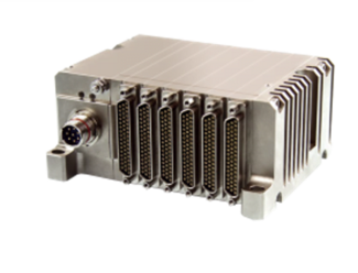
- Designed for Harsh Environments: – 50°C / +105°C, Waterproof, Shocks, Vibration, Lightning, EMI/EMC
- Ultra Compact: Generic analog module, 2×3’’ / 51×76 mm, from 1 to 16 modules per stack
- Best Data Ever: 500 ppm in extreme temperature range
- Easy to Configure: eZ software Suite, XML schema (MDL)
- INET Ready: UDP communication, IEEEE1588 synchronization, SNMP
- Multi Format Output Stream: PCM Chapter 4, Chapter 7, Chapter 10, UDP, IENA, DAR
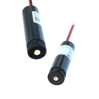
- Universal mini pointer
- Manual focusing optics
- Optical output power from 1mW to 5mW
- Electrically isolated housing (green)
- 5 to 24VDC supply voltage with reverse polarity protection
- Wavelength 635nm (red) or 520nm (green
The ZF-pe-F is an ultra-compact dot laser module with a diameter of only 11 mm, making it easy to integrate into space-limited machine setups. Manual focusing allows the laser to be perfectly adjusted for any working distance, ensuring maximum flexibility in use. With a wavelength of 635 nm (red) or optionally 520 nm (green), it delivers excellent visibility on a wide range of materials. Electrically isolated and equipped with a wide 5–24 VDC supply range including reverse-polarity protection, the module is available with output powers from 1 to 5 mW. Typical applications include woodworking, stone processing, textiles, metal, tire, concrete, and food industries where compact precision is essential.

Superior Mechanics
- Highly stable granite base
- Independent, coarse movement of X and Y axes, combined with easy fine adjustments
- Excellent measurement accuracy and repeatability
- Fast navigation and high-precision probe positioning
See "Specifications & Details" tab for more key features
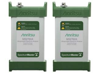
- First portable spectrum analyzer to provide continuous frequency coverage to 170 GHz
- Broadband mmWave capabilities for radio astronomy, automotive radar, wireless backhaul, 802.11ad, satcom, and more
- Ultraportable form factor enables measurements right at the device under test
- Measure: channel power, adjacent channel power, occupied bandwidth
- Patented NLTL technology provides > 100 dB dynamic range
- -141/-136/-129/-122 dBm DANL to 90/110/145/170 GHz ( Spectrum Master MS2762A)
- Up to 6 traces, 3 trace detectors, and 12 markers
- Standard three-year warranty
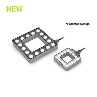
Engineered for critical hygienic environments, the RL322 Series UltraSeal™ Ring Light provides rugged bright field illumination in 50mm and 100mm camera opening sizes. Achieving 3rd-party IP69K certification, these lights ensure complete protection against high-pressure, high-temperature steam cleaning.
Their patented, virtually crevice-free design eliminates exposed fasteners to prevent bacteria buildup and simplifies cleaning. This hygienic construction makes them ideal for direct installation in Food & Beverage splash zones, ensuring reliable performance despite constant exposure to liquid, food debris, and rigorous sanitation protocols. Available in Stainless Steel or Anodized Aluminum to suit specific caustic resistance needs, the RL322 Series can be paired with autoVimation’s IP69K Dolphin camera enclosures (an Exaktera family product) for a more complete, sanitary machine vision imaging solution.

-
Ease of use – Less experienced operators can perform DC measurements by simply pushing a button. This reduces the need of experienced users full time on each system.
-
Reduced Soak Time – The system will automatically re-align the probes to the pads if they drift from alignment. This reduces test time and increases throughput.
-
Unattended Use – Measurements can be left running over night or the weekend, testing all devices on the wafer, and at different temperatures without the need of an operator.

- Light-tight version and EMI-shielded version for low noise and light-sensitive measurements
- Application flexibility, ideal for use in high frequency applications
- Sized to accommodate thermal chucks, laser cutter, and video equipment on the probe system
- Suitable for integration with vibration isolating tables

- Ideal for multiport RF/Microwave and high-speed digital signal testing
- Mix DC and RF/Microwave signals on one probe
- Long lifetime – typically over one million (1,000,000) touchdowns
- Excellent performance in temperatures ranging from 10 K to 200°C
- Probe on any pad material with no damage
FormFactor, Inc.
Website
FormFactor, Inc. (NASDAQ:FORM) is a leading provider of essential test and measurement technologies along the full IC life cycle – from characterization, modeling, reliability, and design de-bug, to qualification and production test.
We constantly strive to help our customers solve the advanced test and measurement challenges of the broader semiconductor industry. Our focus on customer partnership, innovation, agility and operational excellence allows us to earn sustainable business every day.
 - Enabling single-contact high-current/high-voltage test")