You design the future. We help you make it happen.
FormFactor - Cascade Unity Probe - Multicontact probe for RFIC engineering test
- Up to 12 contacts; any contact can be DC, Power, Logic to 500 MHz,or RF to 20 GHz
- Online design configuration tool helps you to specify your probe in minutes
- All designs are fully quadrant compatible
- Full solution includes probes, calibration substrates, stations, accessories and software
- Scalable architecture for future needs
The multi-contact Unity Probe provides highly flexible configurability, unprecedented durability and ease-of use for RFIC engineering test. Unlike “bent-to-order” needle-probe solutions, Unity probes are quickly “built-to-order” with a precision tip cluster featuring multiple independently compliant fingers to isolate chip components from probing stresses — maximizing probe life and durability. Each contact can be configured to one or several contact types and frequencies, and the Unity Probe delivers on the legendary quality you’ve come to expect from our comprehensive suite of probing solutions.
Use our online tool to capture your design requirements and receive a quote.
More Product Information

PureLine 3 Technology
- Provides an effectively noise free environment around the device under test (DUT)
- First automated probe station to achieve -190dB spectral noise*
- Up to 32x lower noise (1kHz), for improved device characterization and modelling at the 7/5/2 nm technology nodes targeted for 5G and beyond applications
- Eliminates over 97% of the environmental noise experienced in previous probe systems
- Extensive collection of FormFactor patents, electrical design knowledge, and measurement system IP
Plug In and Go
- World’s first probe station with integrated TestCell Power Management (a TestCell is a connected set of equipment, including test software, instruments, probe station, thermal system, and related measurement accessories such as cables and on-wafer probes)
- Eliminates all ground-loop induced TestCell noise
- Low field emissions
- Provides fully managed and filtered AC power to the entire system, prober and instruments
See "Specifications & Details" tab for more key features

Flexibility
- Different substrate carriers for wafers up to 100 mm or single dies
- Up to six positioners
- Use with liquid nitrogen or helium, depending on the target temperature
- Probing with an open chamber lid possible under atmospheric condition
- Specially designed for laboratory environments
- Covers wide range of measurements (I-V, C-V, RF, MEMS, OPTO)
See "Specifications & Details" tab for more key features

- Power bypass inductance: 8 nH
- Standard DCQ probes have flat tip needles available in nickel-plated tungsten or BeCu with diameters of 0.75 mil, 1.0 mil and 1.5 mil.
- Supports collinear and non-standard needle configurations
- Up to 16 DC for standard; maximum of 24 DC for custom
- Ideal for probing the entire circuit for functional test
- DC probes can provide power or slow logic to circuit under test
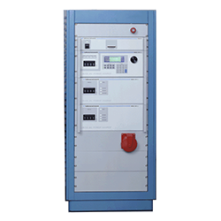
- Comprehensive Test Solutions - Our CTS 4.0 Series offers complete test solutions for emissions and immunity compliance testing of AC and DC power products, ensuring your products are ready for global markets.
- Single & Three Phase Operation - Offers flexibility
- Direct PC Bus Access - Provides high sampling rate and resolution for accurate measurements and high-speed data transfers
- PC-Based Harmonic & Flicker Testing - Provides real-time full-color data display updates and continuous PASS/FAIL monitoring
- Supports Global Standards - Supports European and Japanese standards
- Easy To Use Interface - Provides IEC test setup, data analysis, display, MS Word test reports, and data files generated in MS Excel format
- High Resolution - Data storage to disk for post-acquisition analysis and reporting
- Single Step - Single Step and Fast Forward replay of recorded test data at 200 mSec

- Revolutionary technology advancement for wafer and die-level photonics probing
- Real-time in-situ calibrations
- Singulated die testing
- True die-level edge coupling
- In-situ power measurements
- Advanced calibration technologies
- Enables autonomous measurements
See "Specifications & Details" tab for more key features

SlimVue Microscope
- Combined eye-pieces and CCD camera mount
- 3x zoom and quick lens exchange
- Quick lens exchange
- 1 um optical resolution
- Minimized scope footprint
- Fast change from navigation optics to high-resolution optics
- Resolving ‹ 50 μm pads
- Simple integration with any mmW modules
Application Specific Sigma Kits
- Engraved guides on mmW platen
- Supports broadband, load pull, coax RF and banded waveguide configuration
- Optical feedback on platen position (gauge)
- Adaptable to any mmW/sub-THz applications
- Seamless integration with any mmW modules and tuners
- Fast mounting and setup change
THz measurement capability
- Rock-solid mechanical design
- Submicron stage accuracy
- Optical feedback on platen and probe position (gauge)
- Motorized positioner
- <+-1 um separation repeatability
- Micrometer-accurate and repeatable probe placement and overtravel
- Highly-precise and stable THz measurements
- Mechanical Platen Lift: Enhances safety during complex RF set-ups, increasing operator confidence and minimizing the risk of errors.
- Ease of Use and Advanced Automation: Fully compatible with FormFactor’s Autonomous RF and DC measurement assistants, as well as Velox Dash™ companion app control.
- Reconfigurable Platen Inserts: Quickly switch between TopHat, PCH, and IceShield inserts within minutes to support a wide variety of test configurations.
- Spacious Platen Design: Provides flexibility for both RF and DC setups without space limitations, ensuring easy integration of different configurations.
- Compact Design: Small footprint with field-upgradable components for smooth integration into existing test cells.
- Low-Volume MicroChamber and FemtoGuard Thermal Triaxial Chuck: Included by default
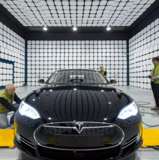
Specific application to Automotive.
The Gold standard for EMC Anechoic Chambers, this 10 meter test range ensures EMC compliance testing Emission and Immunity testing and is compliant to ANSI C63.4/CISPR-16-1-4 with a Test Volume diameter of 4 meters or greater. The most versatile and accurate of EMC test chambers. Ferrite tiles and hybrid pyramidal absorbers allow for high accuracy and performance while meeting compact space requirements.

- Tests and validates performance directly on silicon without post-dicing packaging
- Dramatically reduces time to data and shortens development cycles
- Enables high scalability for high volume manufacturing
- Offers flexibility in chip design with full grid probing
FormFactor, Inc.
Website
FormFactor, Inc. (NASDAQ:FORM) is a leading provider of essential test and measurement technologies along the full IC life cycle – from characterization, modeling, reliability, and design de-bug, to qualification and production test.
We constantly strive to help our customers solve the advanced test and measurement challenges of the broader semiconductor industry. Our focus on customer partnership, innovation, agility and operational excellence allows us to earn sustainable business every day.
