Probes
Products
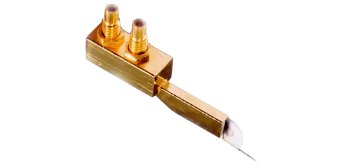
- Ultra-low, fA-level current and fF-level capacitance measurements from -65 °C to + 300 °C
- Guarantees fully-guarded measurements to fA and fF levels
- Individual connectors provide force-sense connection for quasi-Kelvin and CV measurements
- Allows probing of different pad materials and sizes
- Fast replacement of worn probes without the need for tools
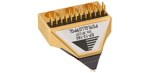
- High performance power bypassing provides low-impedance and resonant-free connections to 20 GHz
- RF bandwidth to 500 MHz
- Long probe life: > 250,000 contacts
- Beryllium-copper tips for gold pads or tungsten for aluminum pads
- Oscillation-free testing of wide-bandwidth analog circuits
- Use with ACP series probes to provide functional at-speed testing for known-good-die
- Mix multiple contact types: Ground, Power (Standard or Eye-Pass), Logic/Signal
- Low and repeatable contact resistance on aluminum pads ( < 0.25 Ω on Al, < 0.01 Ω on Au)
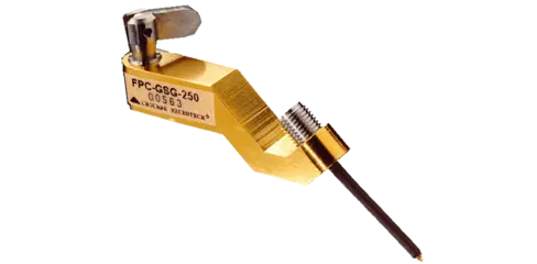
- DC-40 GHz bandwidth
- 10 ps rise time
- Low insertion and return loss
- 2 mils of tip-to-tip compliance
- High probing angle and clearance
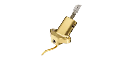
- Enables wafer probing up to 100 A pulsed and 10A DC
- Innovative multi-fingertip design provides even distribution of current
- Supports up to 500 V
- Replaceable Tungsten probe tips
- Temperature range of -60°C to 300°C
- Minimal contact resistance at the pad-tip junction to reduce heating during measurements, with fewer probe marks
- Prevents against thermal runaway
- Measure devices on wafer at higher currents than ever before
- Small scrub minimizes damage to aluminum pad
- Small footprint – tip fits on a 1 mm pad
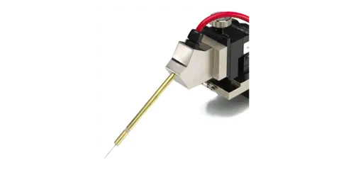
- Coaxial and triaxial measurements up to 10,000 V
- High-quality construction with low-noise electrical performance
- Replaceable probe tips in a variety of tip sizes
- Temperature range of of -60°C to 300°C
- Triaxial measurement ensures a much better understanding of device leakage in the off state
- Highly reliable, stable and repeatable measurements
- Integrally designed as part of a complete measurement solution
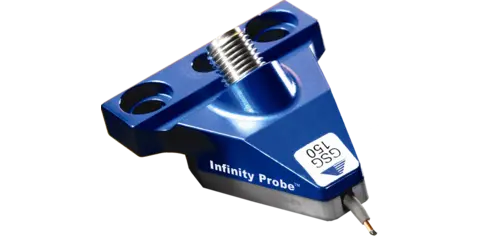
- Lithographic thin-film construction
- Excellent crosstalk characteristics
- Non-oxidizing nickel alloy tips
- Innovative force delivery mechanism
- 40GHz, 50GHz, 67GHz, 110GHz and 145GHz connectors available
- GSG, SG, GS, GSGSG, GSSG, SGS configurations
- 50 to 250 µm pitches (other pitches available on request)
- High current version (2 A) available
Advantages
- Superior field confinement reduces unwanted couplings to nearby devices and transmission modes
- Superior measurement accuracy and repeatability
- Small scrub minimizes damage to aluminum pad
- Typical contact resistance < 0. 05 Ω on Al, <0.02Ω on Au
- Save valuable wafer space and reduce pad parasitics by being able to shrink pad geometries to 25 x 35 µ m (best case)
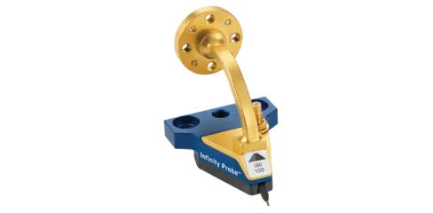
- Probe loss is 3 dB typical between 140 and 200 GHz, S11/S22 15 dB typical
- Reduced unwanted couplings and transmission modes
- Able to shrink pad geometries to 25 x 35 µm (best case)
- Typical contact resistance < 0.05 Ω on Al, < 0.02 Ω on Au
- WR15, WR12, WR10, WR8, WR6, WR4, WR3, and WR2 bands available.
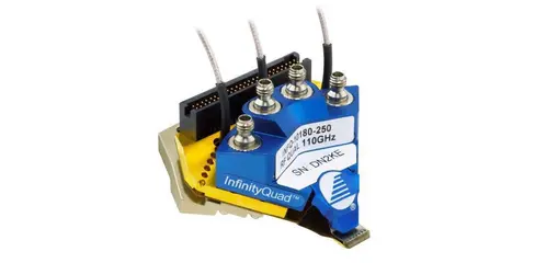
- Customizable configuration up to 25 contacts: RF, Eye-Pass power, ground, logic
- Lithographically-defined tips allow automated over temperature measurement on pads as small as 30 µm x 50 µm
- Low and repeatable contact resistance on aluminum pads (< 0.05 Ω) ensures accurate results
- Durable probe structure ensures more than 250,000 contacts
- Able to measure from -40°C to +125°C without compromising performance or accuracy of specifications
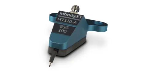
Next Generation Wafer Probing
- Continues the Infinity family’s Industry leading electrical performance
- High temperature capability (175° C +) for automotive device characterization and other applications
- Better tip visibility for enhanced placement accuracy and repeatability
- Improved tip life/durability with solid rhodium contacts
- New tip architecture enables support for narrower pitches (e.g. 25um)
- Advanced mechanical design combined with small contacts enables probing on smaller pads/pitches and improves durability and robustness