You design the future. We help you make it happen.
FormFactor - Cascade Eye-Pass Probe - Durable multi-contact wafer probe with controlled impedance power bypass technology
- High performance power bypassing provides low-impedance and resonant-free connections to 20 GHz
- RF bandwidth to 500 MHz
- Long probe life: > 250,000 contacts
- Beryllium-copper tips for gold pads or tungsten for aluminum pads
- Oscillation-free testing of wide-bandwidth analog circuits
- Use with ACP series probes to provide functional at-speed testing for known-good-die
- Mix multiple contact types: Ground, Power (Standard or Eye-Pass), Logic/Signal
- Low and repeatable contact resistance on aluminum pads ( < 0.25 Ω on Al, < 0.01 Ω on Au)
The multi-contact Eye-Pass probe provides controlled impedance power connections enabling functional testing of even the most challenging circuits on-wafer. The high-durability composite multi-finger tip provides high compliance and ensures precise alignment. This custom probe allows the user to select the footprint pattern best suited for the application, with up to 12 contacts per probe head. Available contact types are ground, logic, standard and Eye-Pass power supply, power supply sense, and ac signal.
Document
More Product Information

Superior Mechanics
- Highly stable granite base
- Independent, coarse movement of X and Y axes, combined with easy fine adjustments
- Excellent measurement accuracy and repeatability
- Fast navigation and high-precision probe positioning
See "Specifications & Details" tab for more key features

- S-parameters DC to 40 GHz, single-ended and mixed-mode
- Impedance Profile with <1 mm resolution, differential and common mode
- Built-in automatic calibration, no manual setup required
- TDR-powered impedance profiling enables precise de-embedding
- Advanced de-embedding including Time Gating and 2Xthru
- Emulate eye diagrams with equalization and advanced jitter analysis
- Complete NRZ and PAM analysis suite for high-speed serial data
- All-in-one solution for testing, compliance, and diagnostics.

Superior Mechanics
- Highly stable granite base
- Independent, coarse movement of X and Y axes, combined with easy fine adjustments down to submicron ranges
- 1 µm repeatable separation stroke
- Excellent measurement accuracy and repeatability
- Fast navigation and high-precision probe positioning
See "Specifications & Details" tab for more key features

- DC-40 GHz bandwidth
- 10 ps rise time
- Low insertion and return loss
- 2 mils of tip-to-tip compliance
- High probing angle and clearance
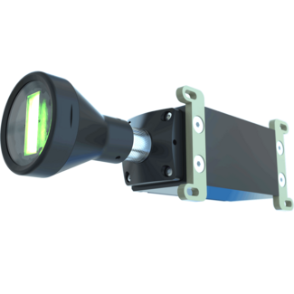
- 600 mW optical output power
- Eye-safe according to laser class 2M
- 70° fan angle
- Connection via 5-pin plug (12-24VDC) or 110-230VAC power supply unit
- Manually focusable
- IP67 RATED
- Integrated TTL Modulation*
The ZQ1-MagicLine is the brightest eye-safe line laser in its class worldwide, setting new standards in industrial laser technology. With its unique combination of laser class 2M safety and 600 mW optical output, it ensures a bright and precise line even in the most challenging lighting conditions. Unlike conventional lasers, it remains clearly visible in bright environments, making it ideal for positioning tasks with widely varying light levels. Its green 520 nm wavelength is especially well perceived by the human eye, while the 70° fan angle creates long, uniform lines. Manual focusing further enhances flexibility, making the ZQ1-MagicLine the perfect solution whenever precision, visibility, and safety must align.

Gold-plated TESLA High-power MicroVac™ Chucks
- Prevent thin wafers from curling and breaking
- Advanced MicroVac chuck surface for minimum contact resistance between wafer and chuck
- Accurate Rds(on) measurement at high current
- Accurate UIS measurements at high temperature
See "Specifications & Details" tab for more key features

Flexibility
- Different substrate carriers for wafers up to 200 mm or single dies
- Probe cards and/or up to eight positioners
- Use with liquid nitrogen or helium, depending on the target temperature. Or use of cryo-cooler for dry-cooling option.
- Accessories available, such as black bodies and optical motion analysis tools
- Optional upgrade for 300 mm wafer
- Designed for industrial environments
- Covers wide range of measurements (I-V, C-V, RF, MEMS, OPTO)
- Ideal for small structures
See "Specifications & Details" tab for more key features

- Power bypass inductance: 8 nH
- Standard DCQ probes have flat tip needles available in nickel-plated tungsten or BeCu with diameters of 0.75 mil, 1.0 mil and 1.5 mil.
- Supports collinear and non-standard needle configurations
- Up to 16 DC for standard; maximum of 24 DC for custom
- Ideal for probing the entire circuit for functional test
- DC probes can provide power or slow logic to circuit under test

Flexibility
- Different substrate carriers for wafers up to 200 mm or single dies
- Probe cards and/or up to eight positioners
- Optional thermal chuck (-60°C to 300°C) and pressure regulation
- Accessories available, such as black bodies and optical motion analysis tools
- Optional upgrade for 300 mm wafer
- Designed for industrial environments
- Covers wide range of measurements (I-V, C-V, RF, MEMS, OPTO)
- Ideal for small structures
See "Specifications & Details" tab for more key features
FormFactor, Inc.
Website
FormFactor, Inc. (NASDAQ:FORM) is a leading provider of essential test and measurement technologies along the full IC life cycle – from characterization, modeling, reliability, and design de-bug, to qualification and production test.
We constantly strive to help our customers solve the advanced test and measurement challenges of the broader semiconductor industry. Our focus on customer partnership, innovation, agility and operational excellence allows us to earn sustainable business every day.
