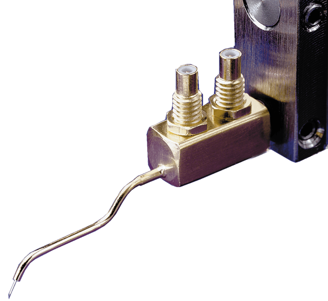
FormFactor - Cascade DCP 100 Series Probe - Delivers superior guarding and shielding
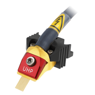
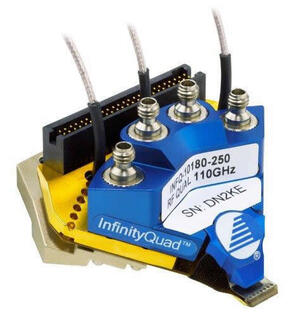
- High-quality construction with low-noise electrical performance
- Kelvin version for convenient 4-point measurements
- Replaceable coaxial probe tips, with choice of tip radii, and full electrical guard to the probe tip
- SSMC 50 connectors
- Ultra-low, fA and fF measurements from -65 º C to 150 º C
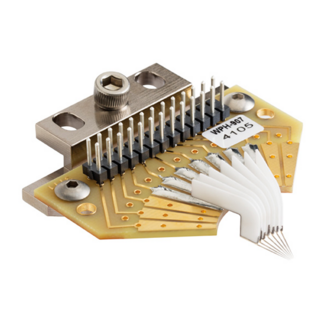
The DCP100 delivers the measurement accuracy needed for advanced on-wafer process, device characterization and reliability testing. With superior guarding and shielding, these probes overcome the performance limitations of non-coaxial needle probes. They are integrally designed as part of a complete measurement solution, these probes are highly reliable, stable and repeatable.
Advantages
- Ultra-low, fA and fF measurements from -65 º C to 150 º C
- Full electrical guard to the probe tip
- Integrally designed as part of Cascade’s complete measurement solution
- Highly reliable, stable and repeatable
More Product Information
- Up to 12 contacts; any contact can be DC, Power, Logic to 500 MHz,or RF to 20 GHz
- Online design configuration tool helps you to specify your probe in minutes
- All designs are fully quadrant compatible
- Full solution includes probes, calibration substrates, stations, accessories and software
- Scalable architecture for future needs

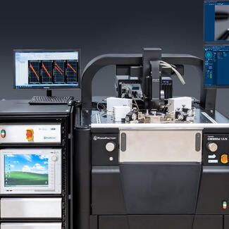
Comprehensive, Turn-key Integrated Measurement System (IMS) with Keysight PDA for On-wafer R&D Power Semiconductor Device Characterization Measurements

Flexibility
- Different substrate carriers for wafers up to 200 mm or single dies
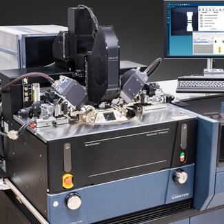
- Probe cards and/or up to eight positioners
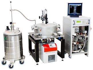
- Use with liquid nitrogen or helium, depending on the target temperature. Or use of cryo-cooler for dry-cooling option.
- Accessories available, such as black bodies and optical motion analysis tools
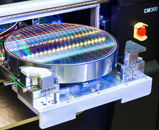
- Optional upgrade for 300 mm wafer
- Designed for industrial environments
- Covers wide range of measurements (I-V, C-V, RF, MEMS, OPTO)
- Ideal for small structures
See "Specifications & Details" tab for more key features

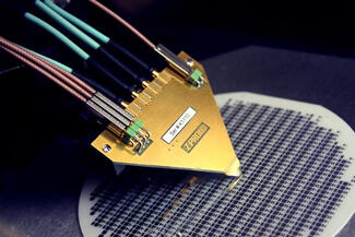
- Revolutionary technology advancement for wafer and die-level photonics probing
- Real-time in-situ calibrations
- Singulated die testing
- True die-level edge coupling
- In-situ power measurements
- Advanced calibration technologies
- Enables autonomous measurements
See "Specifications & Details" tab for more key features

- DC-40 GHz bandwidth
- 10 ps rise time
- Low insertion and return loss
- 2 mils of tip-to-tip compliance
- High probing angle and clearance

-
Ease of use – Less experienced operators can perform an RF calibration up to 500 GHz by simply pushing a button. This reduces the need of experienced users full time on each system.
-
Reduced Soak Time – The system will automatically re-align the probes to the pads if they drift from alignment. This reduces test time and increases throughput.
-
Unattended Use – Measurements can be left running over night or the weekend, testing all devices on the wafer, and at different temperatures without the need of an operator.
-
Calibration Monitor and Re-calibration – System will continuously monitor calibration drift, and automatically re-calibrate the system should the drift exceed a predefined limit.

- High-quality construction with low-noise electrical performance
- Kelvin version for convenient 4-point measurements
- Replaceable coaxial probe tips, with choice of tip radii, and full electrical guard to the probe tip
- SSMC 50 connectors
- Ultra-low, fA and fF measurements from -65 º C to 150 º C

- Probe loss is 3 dB typical between 140 and 200 GHz, S11/S22 15 dB typical
- Reduced unwanted couplings and transmission modes
- Able to shrink pad geometries to 25 x 35 µm (best case)
- Typical contact resistance < 0.05 Ω on Al, < 0.02 Ω on Au
- WR15, WR12, WR10, WR8, WR6, WR4, WR3, and WR2 bands available.

More than a calibration tool
- Calibration
- Validation
- Measurement
- Analysis
No one supports more VNA’s
- Support of more than 24 of the most common VNA’s
Tool for the novice
- Guided wizards and multimedia tutorials integrated
- Intelligence in setups
See "Specifications & Details" tab for more key features

FormFactor, Inc.
FormFactor, Inc. (NASDAQ:FORM) is a leading provider of essential test and measurement technologies along the full IC life cycle – from characterization, modeling, reliability, and design de-bug, to qualification and production test.
We constantly strive to help our customers solve the advanced test and measurement challenges of the broader semiconductor industry. Our focus on customer partnership, innovation, agility and operational excellence allows us to earn sustainable business every day.
Contact Details
FormFactor, Inc. Corporate Headquarters
7005 Southfront Road, Livermore, CA 94551, USA
Phone: 925-290-4000
Test & Measurement