You design the future. We help you make it happen.
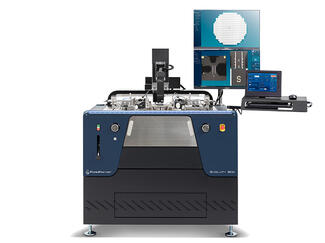
FormFactor - HPD PQ500 - Cryogenic Probe Socket Solution
- Tests and validates performance directly on silicon without post-dicing packaging
- Dramatically reduces time to data and shortens development cycles
- Enables high scalability for high volume manufacturing
- Offers flexibility in chip design with full grid probing
The HPD PQ500, a first-of-its-kind, cryostat-agnostic, high-density RF and DC socket interface, enables researchers and developers to test chips without wire bonding and packaging. The cryogenic probe socket solution can be used at mK temperatures, adaptable to an existing cryostat, accommodating small pitches, and capable of having an extremely high channel capacity.
Document
Document
More Product Information

Flexibility
- Different substrate carriers for wafers up to 200 mm or single dies
- Probe cards and/or up to eight positioners
- Optional thermal chuck (-60°C to 300°C) and pressure regulation
- Accessories available, such as black bodies and optical motion analysis tools
- Optional upgrade for 300 mm wafer
- Designed for industrial environments
- Covers wide range of measurements (I-V, C-V, RF, MEMS, OPTO)
- Ideal for small structures
See "Specifications & Details" tab for more key features

- Probe loss is 3 dB typical between 140 and 200 GHz, S11/S22 15 dB typical
- Reduced unwanted couplings and transmission modes
- Able to shrink pad geometries to 25 x 35 µm (best case)
- Typical contact resistance < 0.05 Ω on Al, < 0.02 Ω on Au
- WR15, WR12, WR10, WR8, WR6, WR4, WR3, and WR2 bands available.

Three Probe Technologies
- Infinity Probe: best for Al (Si)
- ACP Probe: best for AU (III-Vs)
- |Z| Probe: robust solution (long lifetime)
- Precision contact on a wide variety of materials from 26 GHz to 67 GHz
- Accurate results with excellent crosstalk
- Matching cables and substrates included
Precise Contact Solution
- RF chuck ±3 μm surface planarity
- Unique 500 μm platen contact/ separation stroke with ≤± 1 μm accuracy for repeatable contact
- Precision probe alignment
- Consistent contact force and overtravel
- Stable contact performance
WinCal Calibration Software
- Exclusive 1-, 2-, 3-, and 4-port on-wafer calibration algorithms
- Automated calibration monitoring
- Unique measurement & analysis methods
- Accurate S-parameter measurements
- Automatic calibration setup for higher efficiency
- Fast and easy data interpretation and reporting

PureLine 3 Technology
- Provides an effectively noise free environment around the device under test (DUT)
- First automated probe station to achieve -190dB spectral noise*
- Up to 32x lower noise (1kHz), for improved device characterization and modelling at the 7/5/2 nm technology nodes targeted for 5G and beyond applications
- Eliminates over 97% of the environmental noise experienced in previous probe systems
- Extensive collection of FormFactor patents, electrical design knowledge, and measurement system IP
Plug In and Go
- World’s first probe station with integrated TestCell Power Management (a TestCell is a connected set of equipment, including test software, instruments, probe station, thermal system, and related measurement accessories such as cables and on-wafer probes)
- Eliminates all ground-loop induced TestCell noise
- Low field emissions
- Provides fully managed and filtered AC power to the entire system, prober and instruments
See "Specifications & Details" tab for more key features

- Revolutionary technology advancement for wafer and die-level photonics probing
- Real-time in-situ calibrations
- Singulated die testing
- True die-level edge coupling
- In-situ power measurements
- Advanced calibration technologies
- Enables autonomous measurements
See "Specifications & Details" tab for more key features

Flexibility
- Different substrate carriers for wafers up to 150 mm or single dies
- Up to six positioners
- Optional thermal chuck (-60°C to 300°C) and pressure regulation
- Probing with an open chamber lid possible under atmospheric condition
- Specially designed for laboratory environments
- Covers wide range of measurements (I-V, C-V, RF, MEMS, OPTO)
See "Specifications & Details" tab for more key features

Flexibility
- Ideal for a wide range of applications such as RF, mm-Wave and sub-THz characterization, FA, DWC, MEMS, optoelectronic tests and WL
- Re-configurable and upgradable as requirements grow
- Minimizes setup times with no loss in performance or accuracy
- Seamless integration of various measurement instruments
Stability
- Solid station frame
- Built-in vibration-isolation solution for superior vibration attenuation
- Rigid microscope bridge
- Compact and rigid mechanical design
- Highly accurate measurement results
- Incorporates best-known methods
Ease of Use
- Ergonomic and straightforward design for comfortable and easy operation
- Low-profile design
- Simple microscope operation
- Quick and ergonomic change of DUT through pull-out stage
- Minimize training efforts
- Fast time to data
- Convenient operation
- Mechanical Platen Lift: Enhances safety during complex RF set-ups, increasing operator confidence and minimizing the risk of errors.
- Ease of Use and Advanced Automation: Fully compatible with FormFactor’s Autonomous RF and DC measurement assistants, as well as Velox Dash™ companion app control.
- Reconfigurable Platen Inserts: Quickly switch between TopHat, PCH, and IceShield inserts within minutes to support a wide variety of test configurations.
- Spacious Platen Design: Provides flexibility for both RF and DC setups without space limitations, ensuring easy integration of different configurations.
- Compact Design: Small footprint with field-upgradable components for smooth integration into existing test cells.
- Low-Volume MicroChamber and FemtoGuard Thermal Triaxial Chuck: Included by default

Gold-plated TESLA High-power MicroVac™ Chucks
- Prevent thin wafers from curling and breaking
- Advanced MicroVac chuck surface for minimum contact resistance between wafer and chuck
- Accurate Rds(on) measurement at high current
- Accurate UIS measurements at high temperature
See "Specifications & Details" tab for more key features
FormFactor, Inc.
Website
FormFactor, Inc. (NASDAQ:FORM) is a leading provider of essential test and measurement technologies along the full IC life cycle – from characterization, modeling, reliability, and design de-bug, to qualification and production test.
We constantly strive to help our customers solve the advanced test and measurement challenges of the broader semiconductor industry. Our focus on customer partnership, innovation, agility and operational excellence allows us to earn sustainable business every day.


