You design the future. We help you make it happen.
FormFactor - Cascade Vibration Isolation Tables - Tables from simple to highly sensitive
- Designed for use with specific Probe Systems
- Tables to suit all facility requirements and applications
- Stable probing, even in submicron range
- Granite platen ensures rigidity and temperature stability
- Can be combined with the Shield Enclosures
Full range of vibration isolation tables
Working with increasingly small scales of reference means that any vibration however minimal, even from the equipment itself, will seriously degrade a probe station’s performance. Slight vibrations will cause the probes to jump and miss their contacts and the microscope image will be blurred. Our range of vibration isolation tables includes a simple table for general working conditions as well as specifically designed tables for very sensitive measurements such as in the submicron range.
Document
More Product Information

Superior Mechanics
- Highly stable granite base
- Independent, coarse movement of X and Y axes, combined with easy fine adjustments down to submicron ranges
- 1 µm repeatable separation stroke
- Excellent measurement accuracy and repeatability
- Fast navigation and high-precision probe positioning
See "Specifications & Details" tab for more key features
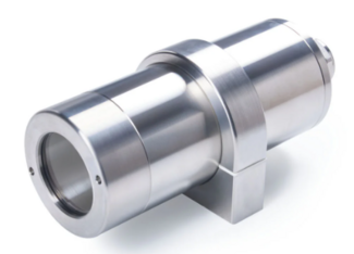
- Electro‐polished V4A stainless steel AISI 316L
- For cameras up to 40 x 40mm cross section
- Robust construction
- Compact size
- High IP protection class
- Flexible camera positioning
- High chemical resistance
- Vibration‐proof mounting
- Camera mount included
- Good heat dissipation
- Easy window replacement

- Enables wafer probing up to 100 A pulsed and 10A DC
- Innovative multi-fingertip design provides even distribution of current
- Supports up to 500 V
- Replaceable Tungsten probe tips
- Temperature range of -60°C to 300°C
- Minimal contact resistance at the pad-tip junction to reduce heating during measurements, with fewer probe marks
- Prevents against thermal runaway
- Measure devices on wafer at higher currents than ever before
- Small scrub minimizes damage to aluminum pad
- Small footprint – tip fits on a 1 mm pad
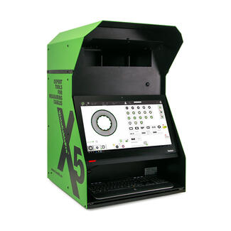
- Object size / measuring range up to 130 mm (5.11“) (larger customizations are possible)
- Quick and very easy measurement
- Little training required (without a customer specified database an initial operating instruction takes only 15 min)
- Suitable software: VELOX (measuring software), ProCable3 (CAQ system)
- Various external CAQ software are connectable (CIQ-AESA, ADVARIS, QDA-ASI-DATAMYTE, QUASAR, etc.)
- No user influence on default optical focus as well as default optimized, intelligent and homogeneous lighting
- Shock and vibration resistant due to an optimized sensor arrangement and balanced weight distribution
- Quick and very precise measurements due to the robust construction and easy operation
- Measuring software enables various operator level settings (production, laboratory, administrator, service, etc.)
- Standardized individual components lead to supply security and therefore a short delivery period
- Easy connection with external devices

- Full-radius, nickel-plated tungsten needles
- Power bypass inductance: 16 nH
- Supports collinear and non-standard needle configurations
- Support up to a maximum of 12 ceramic blades DC needles / contacts
- Ideal for probing the entire circuit for functional test
- DC probes can provide power or slow logic to circuit under test
 - Enabling single-contact high-current/high-voltage test")
FormFactor - Cascade Ultra High-Power (UHP) - Enabling single-contact high-current/high-voltage test
- Enables coaxial measurements up to 10,000 V and 300 A pulsed (600 A in a parallel configuration) with a single touchdown
- Even distribution of high current with innovative multi-fingertip design
- Compatible with TESLA 200/300 mm power device characterization system
- Reduced measurement time by testing both high-voltage and high-current conditions with a single touchdown
- Accurate characterization of a wide range of pad sizes and test currents, with minimum pad damage and contact resistance
- Safe, reliable and repeatable high-current/voltage measurements over a wide temperature range (from -55°C to +300°C)
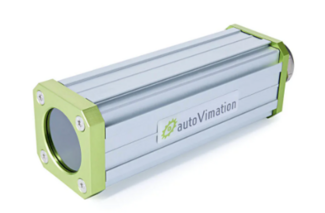
- For cameras up to 40 x 40mm cross section
- Front tube for easy lens access
- Robust construction
- Compact size
- High IP protection class
- Flexible camera positioning
- High chemical resistance
- Vibration‐proof mounting
- Camera mount included
- Excellent heat dissipation

- Up to 12 contacts; any contact can be DC, Power, Logic to 500 MHz,or RF to 20 GHz
- Online design configuration tool helps you to specify your probe in minutes
- All designs are fully quadrant compatible
- Full solution includes probes, calibration substrates, stations, accessories and software
- Scalable architecture for future needs

Flexibility
- Different substrate carriers for wafers up to 100 mm or single dies
- Up to six positioners
- Use with liquid nitrogen or helium, depending on the target temperature
- Probing with an open chamber lid possible under atmospheric condition
- Specially designed for laboratory environments
- Covers wide range of measurements (I-V, C-V, RF, MEMS, OPTO)
See "Specifications & Details" tab for more key features
FormFactor, Inc.
Website
FormFactor, Inc. (NASDAQ:FORM) is a leading provider of essential test and measurement technologies along the full IC life cycle – from characterization, modeling, reliability, and design de-bug, to qualification and production test.
We constantly strive to help our customers solve the advanced test and measurement challenges of the broader semiconductor industry. Our focus on customer partnership, innovation, agility and operational excellence allows us to earn sustainable business every day.
