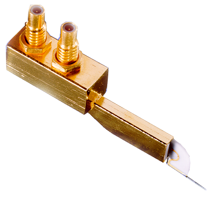
FormFactor - Cascade DCP-HTR Series Probe - High-performance DC parametric probe
-
Ultra-low, fA-level current and fF-level capacitance measurements from -65 °C to + 300 °C
-
Guarantees fully-guarded measurements to fA and fF levels
-
Individual connectors provide force-sense connection for quasi-Kelvin and CV measurements
-
Allows probing of different pad materials and sizes
-
Fast replacement of worn probes without the need for tools
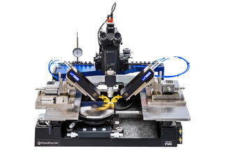
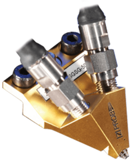
The DCP-HTR probe delivers fA-level measurement capability from -65 °C to 300 °C for advanced characterization and reliability testing. Its unique design offers superior guarding and shielding over-temperature, overcoming the high-temperature performance limitations of standard coaxial needles. When used on a probe station with a MicroChamber, the DCP-HTR allows full utilization of semiconductor parametric test instruments. The optional probe tips with small diameter are ideal for probing pads as small as 30 x 30 μm.
More Product Information

-
Multi-purpose SIGMA instrument integration kit
-
Shorter cabling and universal chuck connection
-
Triax probe with protected guard
-
Triax design for low-leakage measurements up to 3 kV
-
Special chuck surface coating
-
High-isolation ready
-
Arcing protection
-
Shield Enclosure with interlock
-
Advanced grounding concept

-
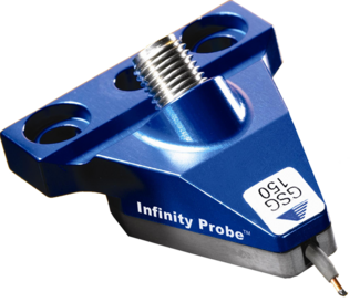
Infinity Probe: best for Al (Si)
-
ACP Probe: best for AU (III-Vs)
-
|Z| Probe: robust solution (long lifetime)
-
RF chuck ±3 μm surface planarity
-
Unique 500 μm platen contact/ separation stroke with ≤± 1 μm accuracy for repeatable contact
-
Exclusive 1-, 2-, 3-, and 4-port on-wafer calibration algorithms
-
Automated calibration monitoring

-
Different substrate carriers for wafers up to 200 mm or single dies
-
Probe cards and/or up to eight positioners
-
Probe positioners placed inside vacuum chamber
-
Short and stable probe arms
-
Joystick controller
-
Manual probe positioners with rotary feed-throughs
-
Software control of chuck for fast step-and-repeat testing of the entire wafer
-
Fast step-and-repeat testing of the whole wafer
-
User-centered design minimizes training costs and enhances efficiency

-
Easy and fast setup of camera views
-
Go to Light and Image Settings of the selected camera view with only one mouse click
-
Guided workflows for wafer setups, alignment tools and Autonomous Assistants
-
Workflow wizard shows task-relevant settings and options only
-
Visualizes the progress of setup, alignment and measurement tasks
-
Status information always at hand
-
Informs the user about events, for example “Successful Alignment”
-
Interacts with the user and helps with intelligent solutions
-
For very complex wafer structures
-
Enables automatic test of multiple devices in each die location before stepping to the next die

-
Different substrate carriers for wafers up to 200 mm or single dies
-
Probe cards and/or up to eight positioners
-
Probe positioners placed inside vacuum chamber
-
Short and stable probe arms
-
Intuitive, manual drives
-
Front loading capability through load door
-
Software control of chuck for fast step-and-repeat testing of the entire wafer
-
Fast step-and-repeat testing of the whole wafer

-
Combination of DC and RF in a single probe module: One dual probe or a maximum of three RF; a maximum of 9 DC standard (other quantities upon request).
-
Utilizes ACP tip design, GSG, GS or SG
-
RF tips available from DC to 110 GHz
-
Choice of BeCu or tungsten tips
-
DC power needles come standard with 100 pF microwave capacitor
-
Power bypass inductance: 8 nH
-
Maximum DC voltage: 50 V without power bypassing (25 V with standard power bypassing, and component dependent with custom power bypassing)
-
Ideal for probing the entire circuit for functional test
-
Dual ACP configuration supports differential signaling applications
-
DC probes can provide power or slow logic to circuit under test

-
Substrate material: High-resistivity silicon
-
Substrate thickness: 275 µm
-
Dielectric constant: 11.8
-
Nominal Z0: 50 Ω

-
On-wafer power device characterization up to 10,000 V DC / 600 A
-
Safe and convenient integration kits to support T.I.P.S. “LuPo” High Voltage / High Power Probe Cards
-
Prevent thin wafers from curling and breaking
-
Safety interlock system with clear enclosure for operator safety during device measurements
-
Convenient connection kits for easy and safe system integration with power device analyzers from Keysight Technologies and major suppliers
-
Up to 25% lower air consumption (CDA) than other systems in the market (300l/min) with no compromise in transition times
-
Windows 10 compatibility enables highest performance and safe operation with state-of-the-art hardware

-
Fully isolated experiment space for true 4K temperatures during probing
-
Cryogenic positioners to provide large travel ranges without warming up the device
-
Flexible thermal jumpers to ensure high thermal conductance and low mechanical transmission
-
A soft vacuum bellows provides a compliant mounting interface for the cryocooler
-
Quick release vacuum feedthroughs for easy configurability
-
A large rectangular port for high signal capacity

FormFactor, Inc.
FormFactor, Inc. (NASDAQ:FORM) is a leading provider of essential test and measurement technologies along the full IC life cycle – from characterization, modeling, reliability, and design de-bug, to qualification and production test.
We constantly strive to help our customers solve the advanced test and measurement challenges of the broader semiconductor industry. Our focus on customer partnership, innovation, agility and operational excellence allows us to earn sustainable business every day.
Contact Details
FormFactor, Inc. Corporate Headquarters
7005 Southfront Road, Livermore, CA 94551, USA
Phone: 925-290-4000
Test & Measurement