You design the future. We help you make it happen.
FormFactor - Cascade DC-Q Probe - Multi-contact DC probe with flat tip needles
- Power bypass inductance: 8 nH
- Standard DCQ probes have flat tip needles available in nickel-plated tungsten or BeCu with diameters of 0.75 mil, 1.0 mil and 1.5 mil.
- Supports collinear and non-standard needle configurations
- Up to 16 DC for standard; maximum of 24 DC for custom
- Ideal for probing the entire circuit for functional test
- DC probes can provide power or slow logic to circuit under test
The DCQ probes use controlled impedance, ceramic blade needles for low noise and high performance. This needle style allows the placement of high-quality bypass capacitors with very little series inductance due to their close proximity to the probe tip. All of the needles are connected to a common ground plane but individual needles can be easily (ground) isolated for additional low noise performance. A maximum of 16 needles are available for standard configurations and a maximum of 24 needles for custom configurations.
More Product Information
")
Differential active probes are like two probes in one. Instead of measuring a test point in relation to a ground point (like single-ended active probes), differential probes measure the difference in voltage of a test point in relation to another test point
 - Enabling single-contact high-current/high-voltage test")
FormFactor - Cascade Ultra High-Power (UHP) - Enabling single-contact high-current/high-voltage test
- Enables coaxial measurements up to 10,000 V and 300 A pulsed (600 A in a parallel configuration) with a single touchdown
- Even distribution of high current with innovative multi-fingertip design
- Compatible with TESLA 200/300 mm power device characterization system
- Reduced measurement time by testing both high-voltage and high-current conditions with a single touchdown
- Accurate characterization of a wide range of pad sizes and test currents, with minimum pad damage and contact resistance
- Safe, reliable and repeatable high-current/voltage measurements over a wide temperature range (from -55°C to +300°C)
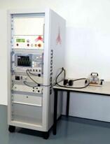
- Automatic calibration for the whole test frequency range
- Application of all test frequencies automatically. The level can be selected or automatic.
- NO need to manually configure the measurement equipment
- NO need to manually integrate the transfer function of probes and attenuators
- Generation of test reports: NO need to record all values read from the measurement equipment
- Generation of calibration reports: NO need to record all calibration setting parameters
- Rack together and add CS101, CS109, and RS101 (sections 18, 19, and 20 of the RTCA DO-160G are also available.)

- High-quality construction with low-noise electrical performance
- Kelvin version for convenient 4-point measurements
- Replaceable coaxial probe tips, with choice of tip radii, and full electrical guard to the probe tip
- SSMC 50 connectors
- Ultra-low, fA and fF measurements from -65 º C to 150 º C

Cryogenic Temperatures
- Fully isolated experiment space for true 4K temperatures during probing
- Cryogenic positioners to provide large travel ranges without warming up the device
- Integrated helium pot for high temperature stability of the device under test
- Fully dry cryogen-free cooler eliminates the need for expensive helium circulation systems
- Rapid cool liquid nitrogen option for faster cool down times
See "Specifications & Details" tab for more key features

Flexibility
- Different substrate carriers for wafers up to 150 mm or single dies
- Up to six positioners
- Optional thermal chuck (-60°C to 300°C) and pressure regulation
- Probing with an open chamber lid possible under atmospheric condition
- Specially designed for laboratory environments
- Covers wide range of measurements (I-V, C-V, RF, MEMS, OPTO)
See "Specifications & Details" tab for more key features

- Customizable configuration up to 25 contacts: RF, Eye-Pass power, ground, logic
- Lithographically-defined tips allow automated over temperature measurement on pads as small as 30 µm x 50 µm
- Low and repeatable contact resistance on aluminum pads (< 0.05 Ω) ensures accurate results
- Durable probe structure ensures more than 250,000 contacts
- Able to measure from -40°C to +125°C without compromising performance or accuracy of specifications

- Revolutionary technology advancement for wafer and die-level photonics probing
- Real-time in-situ calibrations
- Singulated die testing
- True die-level edge coupling
- In-situ power measurements
- Advanced calibration technologies
- Enables autonomous measurements
See "Specifications & Details" tab for more key features

- Tests and validates performance directly on silicon without post-dicing packaging
- Dramatically reduces time to data and shortens development cycles
- Enables high scalability for high volume manufacturing
- Offers flexibility in chip design with full grid probing
FormFactor, Inc.
Website
FormFactor, Inc. (NASDAQ:FORM) is a leading provider of essential test and measurement technologies along the full IC life cycle – from characterization, modeling, reliability, and design de-bug, to qualification and production test.
We constantly strive to help our customers solve the advanced test and measurement challenges of the broader semiconductor industry. Our focus on customer partnership, innovation, agility and operational excellence allows us to earn sustainable business every day.
