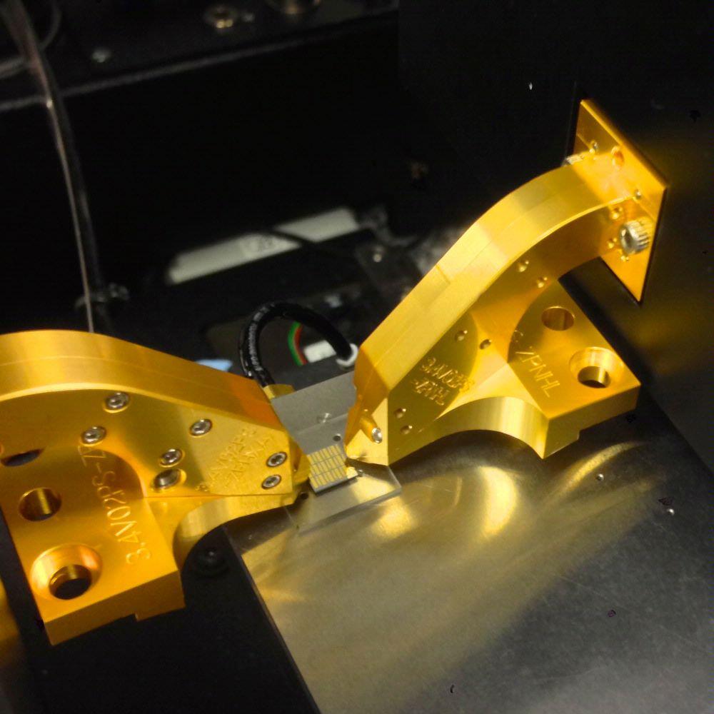
FormFactor - Cascade Multiline TRL Cal Substrates - Multiline TRL substrates for T-Wave probes
- Substrate material: High-resistivity silicon
- Substrate thickness: 275 µm
- Dielectric constant: 11.8
- Nominal Z0: 50 Ω
Millimeter- and submillimeter-wave calibration substrates, optimized for T-Wave™ probes. The multiline TRL calibration substrates offer CPW standards including reflect (short), thru and two lines and are recommended to use with WinCal™ calibration software. Some off-set short and off-set open structures are included for additional measurements.
Models
|
Part Number |
Description |
Pitch (μm) |
|---|---|---|
|
Multi-line TRL Substrate, WR1.0, WR2.2, WR3.4, WR4.3, WR5.1 |
25 |
|
|
Multi-line TRL Substrate, WR2.2, WR3.4, WR4.3, WR5.1 |
50 |
|
|
Multi-line TRL Substrate, WR3.4, WR4.3, WR5.1 |
75 and 100 |
More Product Information
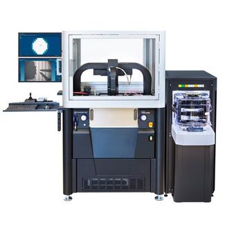
Gold-plated TESLA High-power MicroVac™ Chucks
- Prevent thin wafers from curling and breaking
- Advanced MicroVac chuck surface for minimum contact resistance between wafer and chuck
- Accurate Rds(on) measurement at high current
- Accurate UIS measurements at high temperature
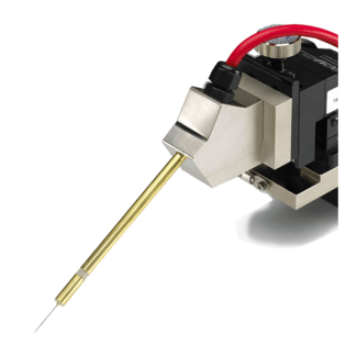
- Coaxial and triaxial measurements up to 10,000 V
- High-quality construction with low-noise electrical performance
- Replaceable probe tips in a variety of tip sizes
- Temperature range of of -60°C to 300°C
- Triaxial measurement ensures a much better understanding of device leakage in the off state
- Highly reliable, stable and repeatable measurements
- Integrally designed as part of a complete measurement solution
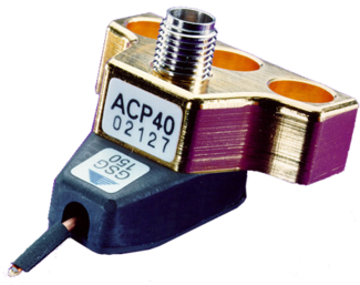
-
Functional temperature range of -263 to +150°C
-
Stainless steel tip material for thermal decoupling
-
Coaxial cable with TCE matched inner and outer conductors
-
Consistent tip geometry even at cryogenic temperatures
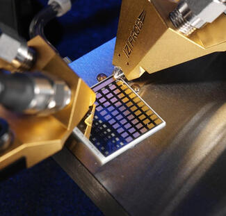
The CSR family of calibration substrates delivers the highest accuracy available due to the high quality of each substrate. The calibration standards are manufactured using rugged, hard gold, which ensures a long lifetime.
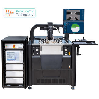
PureLine 3 Technology
- Provides an effectively noise free environment around the device under test (DUT)
- First automated probe station to achieve -190dB spectral noise*
- Up to 32x lower noise (1kHz), for improved device characterization and modelling at the 7/5/2 nm technology nodes targeted for 5G and beyond applications
- Eliminates over 97% of the environmental noise experienced in previous probe systems
- Extensive collection of FormFactor patents, electrical design knowledge, and measurement system IP
Plug In and Go
- World’s first probe station with integrated TestCell Power Management (a TestCell is a connected set of equipment, including test software, instruments, probe station, thermal system, and related measurement accessories such as cables and on-wafer probes)
- Eliminates all ground-loop induced TestCell noise
- Low field emissions
- Provides fully managed and filtered AC power to the entire system, prober and instruments
See "Specifications & Details" tab for more key features
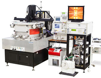
Flexibility
- Different substrate carriers for wafers up to 200 mm or single dies
- Probe cards and/or up to eight positioners
- Use with liquid nitrogen or helium, depending on the target temperature
- Accessories available, such as black bodies and optical motion analysis tools
- Designed for industrial environments
- Covers wide range of measurements (I-V, C-V, RF, MEMS, OPTO)
See "Specifications & Details" tab for more key features
-
Die-to-die stepping time of under 100 ms
-
Up to 20 dies/sec (70,000 dies/hour) with MultiDie Testing technology
-
Even extreme variations in height, such as the case with warped wafers, can be compensated
-
Interfaces to all major analysis instrumentation, optics software and testers
-
Access to top side and bottom side of device under test (DUT)
-
Highly accurate light measurement
-
Test automation out-of-cassette for 24/7 operation
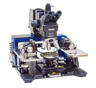
Flexibility
- Ideal for a wide range of applications such as RF, mm-Wave and sub-THz characterization, FA, DWC, MEMS, optoelectronic tests and WL
- Re-configurable and upgradable as requirements grow
- Minimizes setup times with no loss in performance or accuracy
- Seamless integration of various measurement instruments
Stability
- Solid station frame
- Built-in vibration-isolation solution for superior vibration attenuation
- Rigid microscope bridge
- Compact and rigid mechanical design
- Highly accurate measurement results
- Incorporates best-known methods
Ease of Use
- Ergonomic and straightforward design for comfortable and easy operation
- Low-profile design
- Simple microscope operation
- Quick and ergonomic change of DUT through pull-out stage
- Minimize training efforts
- Fast time to data
- Convenient operation
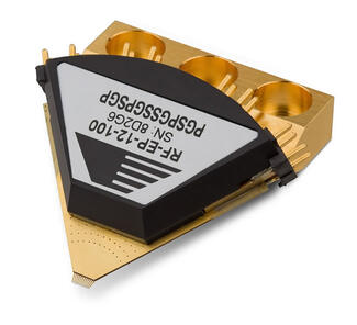
- Up to 12 contacts; any contact can be DC, Power, Logic to 500 MHz,or RF to 20 GHz
- Online design configuration tool helps you to specify your probe in minutes
- All designs are fully quadrant compatible
- Full solution includes probes, calibration substrates, stations, accessories and software
- Scalable architecture for future needs
FormFactor, Inc.
FormFactor, Inc. (NASDAQ:FORM) is a leading provider of essential test and measurement technologies along the full IC life cycle – from characterization, modeling, reliability, and design de-bug, to qualification and production test.
We constantly strive to help our customers solve the advanced test and measurement challenges of the broader semiconductor industry. Our focus on customer partnership, innovation, agility and operational excellence allows us to earn sustainable business every day.
