You design the future. We help you make it happen.
FormFactor - Cascade QuadCard™ - Cost-effective, versatile probe card solution
- Accommodates a combination of up to four Cascade Microtech probes
- Configurable for mixed-signal RF/mmW testing
- Quick and easy repairs to be performed in the field, by simply replacing individual probes
- Adaptable to new device layouts by exchanging individual probes
The QuadCard probe card is the industry’s first configurable, multi-quadrant probe adapter that employs innovative fine probe aligners to mount up to four FormFactor probes on a single probe card. It is designed to accommodate a combination of our probes such as Infinity Probes®, ACP probes, |Z| Probes® and Multi-|Z| Probes, which are aligned individually by the fine probe aligners.
More Product Information

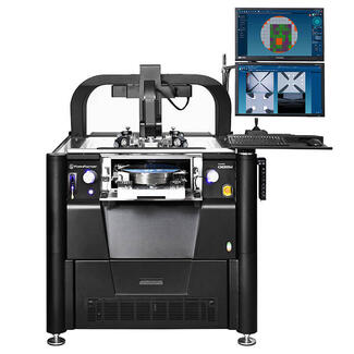
Superior Mechanics
- Highly stable granite base
- Independent, coarse movement of X and Y axes, combined with easy fine adjustments down to submicron ranges
- 1 µm repeatable separation stroke
- Excellent measurement accuracy and repeatability
- Fast navigation and high-precision probe positioning
See "Specifications & Details" tab for more key features

Comprehensive, Turn-key Integrated Measurement System (IMS) with Keysight Photonics Application

Measurement Accuracy
- Best solution for high accuracy IV/CV, low-noise and 1/f measurements with PureLine, AutoGuard and next generation MicroChamber technologies
- Minimize AC and spectral noise with effective shielding capability
- Achieve unsurpassed RF/mmW measurement and calibration accuracy with integrated RF tools and WinCal
- Shortest signal path test integration for accurate, thermally stable, and low-error data collection
See "Specifications & Details" tab for more key features
Flexibility
- DC, AC and RF/microwave device characterization, 1/f, WLR, FA and design debug
- Full thermal range of -60°C to +300°C
- Compatible with TopHat or IceShield
- Usage of manual and motorized positioners, probe cards within EMI-shielded environment
- Upgrade path to meet your future needs
- Stable and repeatable measurements over a wide thermal range
High accuracy and repeatability
- Reliable and repeatable contact
- Moisture-free, light-tight and EMI-shielded test environment with MicroChamber® technology
- Advanced EMI-shielding with PureLine and AttoGuard technologies available
- Superior low-leakage and low-noise measurements
- Safe and accurate hands-off testing
- Minimizes settling times for efficient measurements over full thermal range
See "Specifications & Details" tab for more key features

- Light-tight version and EMI-shielded version for low noise and light-sensitive measurements
- Application flexibility, ideal for use in high frequency applications
- Sized to accommodate thermal chucks, laser cutter, and video equipment on the probe system
- Suitable for integration with vibration isolating tables

Floating Action Buttons
- Easy and fast setup of camera views
- Go to Light and Image Settings of the selected camera view with only one mouse click
Workflow Wizard
- Guided workflows for wafer setups, alignment tools and Autonomous Assistants
- Workflow wizard shows task-relevant settings and options only
- Wizard settings can be corrected anytime – no need to restart the wizard
- Wizard helps with intelligent solutions in case of error
See "Specifications & Details" tab for more key features

Flexibility
- Different substrate carriers for wafers up to 200 mm or single dies
- Probe cards and/or up to eight positioners
- Use with liquid nitrogen or helium, depending on the target temperature
- Accessories available, such as black bodies and optical motion analysis tools
- Designed for industrial environments
- Covers wide range of measurements (I-V, C-V, RF, MEMS, OPTO)
See "Specifications & Details" tab for more key features

- High performance power bypassing provides low-impedance and resonant-free connections to 20 GHz
- RF bandwidth to 500 MHz
- Long probe life: > 250,000 contacts
- Beryllium-copper tips for gold pads or tungsten for aluminum pads
- Oscillation-free testing of wide-bandwidth analog circuits
- Use with ACP series probes to provide functional at-speed testing for known-good-die
- Mix multiple contact types: Ground, Power (Standard or Eye-Pass), Logic/Signal
- Low and repeatable contact resistance on aluminum pads ( < 0.25 Ω on Al, < 0.01 Ω on Au)

Comprehensive, Turn-key Integrated Measurement System (IMS) with Keysight SPA for On-wafer DC Parametric Measurements
FormFactor, Inc.
Website
FormFactor, Inc. (NASDAQ:FORM) is a leading provider of essential test and measurement technologies along the full IC life cycle – from characterization, modeling, reliability, and design de-bug, to qualification and production test.
We constantly strive to help our customers solve the advanced test and measurement challenges of the broader semiconductor industry. Our focus on customer partnership, innovation, agility and operational excellence allows us to earn sustainable business every day.
