Products
Displaying 25 - 36 of 84
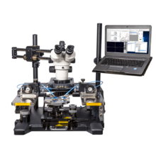
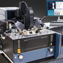
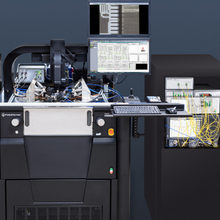
Probe station
Keysight Streamline Vector Network Analyzer (option up to 53 GHz)
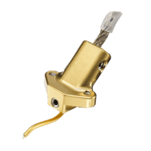
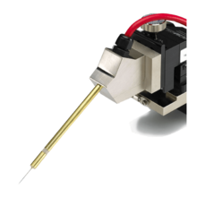
Choice of probes
Known measurement accuracy traced back to independent standards
Enables wafer probing up to 100 A pulsed and 10A DC
Innovative multi-fingertip design provides even distribution of current
Supports up to 500 V
Replaceable Tungsten probe tips
Coaxial and triaxial measurements up to 10,000 V
High-quality construction with low-noise electrical performance
Replaceable probe tips in a variety of tip sizes
Temperature range of -60°C to 300°C
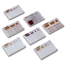
Impedance Standard Substrates (ISSs) supports all of your high-frequency probing applications. Using them ensures greater accuracy and better repeatability in on-wafer calibration of vector network analyzers. Our ISSs offer the proven accuracy of LRRM calibrations with automatic load inductance compensation.
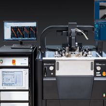
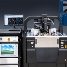
Comprehensive, Turn-key Integrated Measurement System (IMS) with Keysight SPA for On-wafer DC Parametric Measurements
Comprehensive, Turn-key Integrated Measurement System (IMS) with Keysight A-LFNA for On-wafer R&D Advanced Low-Frequency Noise Measurements
Comprehensive, Turn-key Integrated Measurement System (IMS) with Keysight PNA for On-wafer R&D Measurements from RF to millimeter wave to Terahertz
Comprehensive, Turn-key Integrated Measurement System (IMS) with Keysight PDA for On-wafer R&D Power Semiconductor Device Characterization Measurements
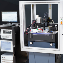
Comprehensive, Turn-key Integrated Measurement System (IMS) with Keysight Photonics Application
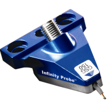
Superior field confinement reduces unwanted couplings to nearby devices and transmission modes
Superior measurement accuracy and repeatability
Small scrub minimizes damage to aluminum pad
Typical contact resistance < 0. 05 Ω on Al, <0.02Ω on Au
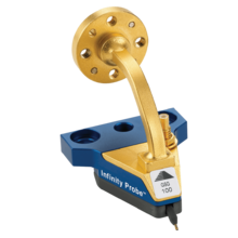
Probe loss is 3 dB typical between 140 and 200 GHz, S11/S22 15 dB typical
Reduced unwanted couplings and transmission modes
Able to shrink pad geometries to 25 x 35 µm (best case)
Typical contact resistance < 0.05 Ω on Al, < 0.02 Ω on Au
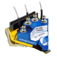
Customizable configuration up to 25 contacts: RF, Eye-Pass power, ground, logic
Lithographically-defined tips allow automated over temperature measurement on pads as small as 30 µm x 50 µm
Low and repeatable contact resistance on aluminum pads (< 0.05 Ω) ensures accurate results
