You design the future. We help you make it happen.
Products
Displaying 409 - 420 of 901
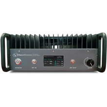
Not all amplifiers are created equal, so how can you be certain that an amplifier will work for your needs? You deserve to be confident that the amplifiers used with your test-and measurement lab benches will meet the requirements of your specific applications, are reliable, and are equally well-supported pre-and post-sale. When it comes to application expertise, reliability and support, there is no company that does it better than Maury.
Not all amplifiers are created equal, so how can you be certain that an amplifier will work for your needs? You deserve to be confident that the amplifiers used with your test-and measurement lab benches will meet the requirements of your specific applications, are reliable, and are equally well-supported pre-and post-sale. When it comes to application expertise, reliability and support, there is no company that does it better than Maury.
Not all amplifiers are created equal, so how can you be certain that an amplifier will work for your needs? You deserve to be confident that the amplifiers used with your test-and measurement lab benches will meet the requirements of your specific applications, are reliable, and are equally well-supported pre-and post-sale. When it comes to application expertise, reliability and support, there is no company that does it better than Maury.
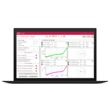
Flexible bench configuration empowers users to easily set up instruments and DUTs to match any measurement workflow.
Automated, multi-instrument calibration workflows empower users to achieve high accuracy results across diverse setups with minimal user intervention.
Built-in system calibration verification instills confidence in measurement accuracy before data collection begins.
Comprehensive small-signal, large-signal, and pulsed testing captures real-world device behavior for reliable design and modeling.
Powerful visualization and analytics suite empowers users to quickly interpret results, extract models, and drive faster design decisions.
Custom electrical testing available upon request
Wide package variety with custom configurations
NC100 & 200 series for audio and RF applications
NC300 & 400 series for microwave application
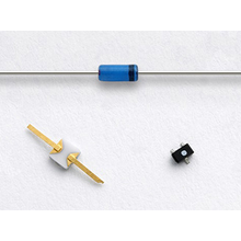
Noise diodes are the fundamental building blocks for analog noise systems. They are categorized for performance characteristics that enhance their broadband noise output and flat spectral response. All Maury noise diodes can deliver symmetrical white Gaussian noise and flat output power versus frequency*.
* Flatness and output power are dependent upon peripheral circuit characteristics
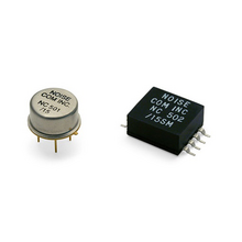
Complete bias circuits
Requires no external components
Extremely flat output power versus frequency characteristics
The NC500 (through-hole) and NC500SM (surface mount) Series noise modules are an economical solution for built-in test requirements. They contain complete bias circuits and require no external components. Some models contain additional gain stages for high power ENR output (51 dB). The surface mount package is suitable for mounting on micro strip. The modules have extremely flat output power versus frequency characteristics that are insensitive to temperature and voltage variations.
Complete bias circuits
Requires no external components
Optimizations available for frequency range and output levels
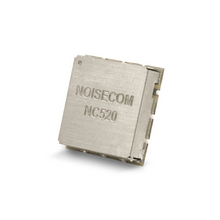
The NC520 low voltage (surface mount) noise module is an economic solution for built-in test requirements. It contains complete bias circuits and require no external components.
The surface mount package is suitable for mounting on microstrip. The modules produce extremely flat output power versus frequency characteristic that is insensitive to temperature and voltage variations.
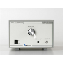
Additive white Gaussian noise
Integrated amplifier
Manual attenuator
NC6000A -BER testing, and SNR applications
NC8000A – Secure signal jamming
Military Applications
Custom configurations available (consult factory)
The NC6000A and NC8000A Series instruments are designed for general-purpose noise applications on the bench, or in a rack test station. The manual controls make it simple to operate and reduce test set up time. Standard units can be modified for specific customer requirements. Please consult the factory for pricing and availability of these requests.
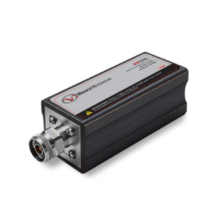
The overall performance of a power meter dependents on the power sensor employed. Maury has a variety of quality power sensors to meet virtually all applications. Maury has a complete line of Peak and Average power sensors up to 40 GHz for all of your fast rise time, wide bandwidth and wide dynamic range applications. In this document, browse through our large variety of advanced sensor solutions.
Automated Absolute and Additive (Residual) Measurements
Real Time Cross Correlation
Only analyzer available that allows actual noise floor measurement
Unparalleled analog performance
Repeatable data
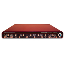
The HA7162C Real Time Phase Noise Analyzer is the industry leader with respect to proven accuracy, high reliability, automation and flexibility; offering extremely fast measurement speeds to reduce product development time and/or optimize ATE manufacturing throughput.
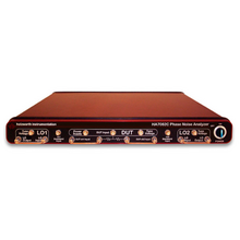
Automated Absolute and Additive (Residual) Measurements
Real Time Cross Correlation
Only analyzer available that allows actual noise floor measurement
Unparalleled analog performance
Repeatable data
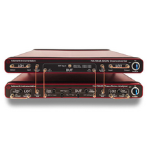
The HA7162D Real Time Phase Noise Analyzer delivers proven accuracy, high reliability, automation and flexibility. The real time engine covers the full measurement bandwidth with extremely fast measurement speeds to reduce product development time and optimizes ATE manufacturing throughput.
Real-Time Full Bandwidth Data Acquisition
Versatile – Reconfigurable Front End
Measure: PM / AM / Baseband / Spurious / Jitter
Isolated AM / PM
Automated Residual Measurements
Outstanding Accuracy
The HA7163A is a heterodyne downconversion system that is designed to seamlessly integrate with Holzworth’s real time phase noise analysis products as a calibrated frequency extension. The HA7163A provides for both absolute and residual (additive) measurements to 50GHz, making it the only solution available on the market for taking accurate additive phase noise measurements at frequencies of greater than 18GHz, without using external mixers.