You design the future. We help you make it happen.
Products
Displaying 421 - 432 of 901
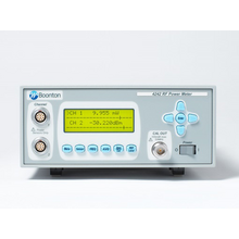
Single or dual-channel display
Agilent HP 437 & Agilent HP 438, and Boonton 4220A & 4230A emulation
Automatically loads sensor data
Simple software control via SCPI language
IEEE-488 and RS-232 interfaces standard
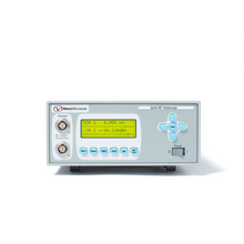
The 4240 series of CW RF power meters provides the high speed measurement capability needed in a production environment, as well as the simplicity of operation required for bench top use. It provides very accurate measurements from -70 dBm to +44 dBm (sensor dependent) and has a rapid display update rate for tuning applications. The easy to read LCD displays both channels simultaneously with numeric and bar graph information.
C/N carrier to noise ratio
C/I carrier to interferer ration
C/No carrier to noise density ratio
Eb/No bit energy to noise density ratio
Custom configurations
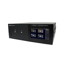
6.25″ color TFT touch screen
Accuracy of 0.2 dB RSS
Bit Rates from 1 bps to 1 Gbs
Variable Output Power from -55 dBm to +5 dBm
Ultra-low distortion signal path
Standard connectors SMA female
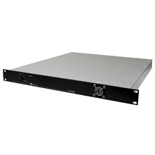
7” touch screen display
Dimensions: 17.22 in. wide x 6.30 in. including feet, high x 19.5 in. deep
Fold-down feet for bench top use
Power 115 VAC, 60 Hz
Operating Temperature: -10° to +65°C
Differential inputs and outputs
Multiple differential inputs and outputs
5” touch screen display
Noise output through female N connector
Ethernet connection for remote control
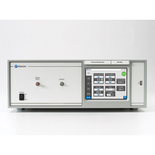
The NGX1000 programmable noise generator is a high performance, broadband additive white gaussian noise (AWGN) generator in an easy-to-use compact form factor. The streamlined user interface and flat menu structure provides a fast, simple way to add RF noise in a communications system to test reliability, robustness and performance.
All functionality of the generator is accessible through the 5” touch screen or via remote control through an ethernet connection delivering flexible, programmable noise generation for broad use in semiconductor, military, aerospace, satellite, medical and communications applications.
Output White Gaussian noise
127 dB of attenuation; 0.1 dB step size
Units > 2 GHz have total attenuation of 79.9 dB
Low distortion signal path
Noise attenuator accuracy:
±0.2 dB or 0.5% at 1 – 500 MHz
±0.2 dB or 1% at 0.5 – 1.0 GHz
±0.3 dB or 2% at 1 – 2 GHz
Standard connectors SMA female
Power 115 VAC, 60 Hz; 110 VAC, 220 VAC
Operating Temperature: -10° to +65°C
Output White Gaussian noise
Output power up to +30 dBm
127 dB of attenuation; 0.1 dB step size
Units > 2 GHz have total attenuation of 79.9 dB
Low distortion signal path
Power 115 VAC, 60 Hz
Noise attenuator accuracy: ±0.2 dB or 0.5% at 1 – 500 MHz ±0.2 dB or 1% at 0.5 – 1.0 GHz ±0.3 dB or 2% at 1 – 2 GHz
Standard connectors SMA female
7” touch screen display
Dimensions: 17.25 in. wide x 6.50 in. including feet, high x 19.50 in. deep
Removable hard drive for added security
Operating Temperature: -10° to +65°C
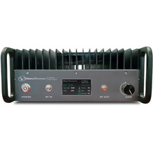
Not all amplifiers are created equal, so how can you be certain that an amplifier will work for your needs? You deserve to be confident that the amplifiers used with your test-and measurement lab benches will meet the requirements of your specific applications, are reliable, and are equally well-supported pre-and post-sale. When it comes to application expertise, reliability and support, there is no company that does it better than Maury.
Not all amplifiers are created equal, so how can you be certain that an amplifier will work for your needs? You deserve to be confident that the amplifiers used with your test-and measurement lab benches will meet the requirements of your specific applications, are reliable, and are equally well-supported pre-and post-sale. When it comes to application expertise, reliability and support, there is no company that does it better than Maury.
Dual-channel and differential voltage measurements
1% accuracy at full scale
True RMS response below 30 mV
Optional low-frequency probe for measurements from 10 Hz to 100 MHz
DC recorder output
IEEE-488 interface standard, RS-232
The 9240 series is the latest addition to the popular 9200 series of RF voltmeters. It combines accuracy, smart probes, and operator features that have never before been available in its price range. It is simple to use on the bench, and comprehensive enough to integrate into an ATE system. Boonton’s proven voltage probes directly measure from 200 μV to 10 V with usable indication as low as 50 μV and have true RMS response below 30 mV.
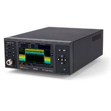
Capture/display/analyze peak and average power
Frequency range from 4 kHz to 40 GHz
Industry-leading video bandwidth (195 MHz) and rise time (3 ns)
Industry-leading 100,000 measurements per second
Industry-leading 100 ps time resolution
Synchronous multi-channel measurements (up to 4 channels)
Sensors can be used as standalone instruments
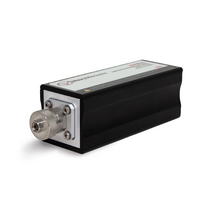
4 kHz to 6 GHz and 10 MHz to 6, 18, and 40 GHz power sensors
-60 dBm to +20 dBm dynamic range
Pulse, Average, CW and Modulation modes
True average measurements with essentially no modulation bandwidth limitations
Real-Time Power Processing™ technology for virtually no gaps in signal acquisition and zero measurement latency
100,000 measurements per second
Synchronized multi-channel measurements
Suite of advanced measurement and analysis software
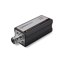
6 GHz, 8 GHz, 18 GHz and 40 GHz RF Power Sensors
Up to 195 MHz video bandwidth with 3 ns rise time
Real-Time Power ProcessingTM technology with zero measurement dead time
100,000 measurements per second
Power Analyzer Suite advanced measurement and analysis software
Crest factor, CCDF and statistical measurements
10 GS/s effective sample rate
100 MS/s continuous sample rate
Synchronized multi-channel measurements